N years of valuable experience tells us that when encountering via stubs, the best way is to route the device on the surface layer to the lower layer, and the device to route the bottom layer to the upper layer, so that the stub can be minimized. However, is there such a situation where you feel that no matter which layer you go to, you feel that the stub cannot be lowered very low?
Well, there really is such an operation, and we actually see a lot of it. In a more ideal device layout, we like to put the high-speed signal transceiver chips on the same side, either on the surface or on the bottom. The reason is very simple. In this case, when we punch holes from the pin on the surface layer to the inner layer, as long as we go to the lower layer (the device is placed on the surface layer, if it is placed on the bottom layer, it is the opposite), so that the two vias are It will be a relatively short via stub, which helps to improve the signal transmission quality. And don't always mention back drilling. It can ensure the quality and save the cost and processing flow simply and quickly. I believe no one will refuse it, right?
However, some high-speed signals can't put both devices on the front, it seems that we don't pay attention to these high-speed wiring. Do you think that as long as we want to ensure their transmission first, we must easily put them on the surface first, right? Some things can’t even be guaranteed by concubines, let alone PCB engineers? For example, one of the devices is a pin with high-speed wiring on both sides...
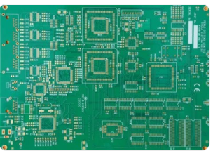
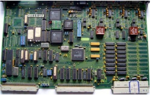
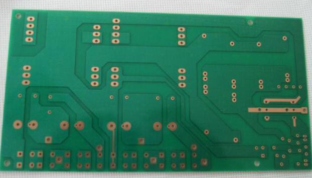
In fact, there are such devices, and they are widely used. One of them is our protagonist today, PCIE gold finger. It is encountered in many of our PCIE daughter card designs. Its package is a double-sided pad structure. We have had a lot of contact with such PCIE signals recently, and they are mainly used in the field of artificial intelligence, which is very popular now.
The highlighted TX link (How to divide TX or RX? Look at the capacitor) is on the bottom layer, and our main chip is placed on the surface layer, so our internal wiring seems to be inaccessible to which layer. The effect when placed on the same side, whether it is placed on the upper layer or the lower layer, there will be one of the vias with a long stub. At this time, I can imagine that the mood of the PCB engineer is as contradictory as the situation in the picture below...
After finishing the previous foreshadowing, let's talk about the case that this article wants to describe. This signal uses the PCIE3.0 protocol (8Gbps), and the board thickness is 2.0mm. In the first edition, in order to save costs, the customer asked us if we could do it without back drilling, and then our high-speed Mr. did not call the customer back drilling at every turn. The stub of the via is about 60mil, which is still acceptable for 8Gbps signals. The customer also voted for the board with a mindset of suspicion, but fortunately, it didn't take long. After returning to the board, the customer conducted a PCIE test (the daughter card was inserted into the base for testing) and found that it was really OK, and there was no problem in transmission.
After everything was okay, the customer later started the second version again, and there were some changes to other wiring, and the PCIE part of the schematic was not changed. It was supposed that PCIE direct copy would be fine, but because the lower traces need to give way to higher-speed signals, it is impossible to continue to trace the bottom layer according to the previous version. At this time, the PCB designer thought that there would be a long via stub anyway, and the impact should be the same, so they put the trace on the upper layer symmetrical to the lower layer, so the second version of the link became like this ( Since the difference between the two will be compared later, it will be more convincing for us to compare the same link with different wiring layers).
This is what I said earlier, no matter whether it is up or down, there will be a long via stub unavoidable. In fact, at first glance, it feels the same, because there is still a long and a short via stub. Is this actually the case?

Let's compare the two cases by simulation, and their transmission loss has a very surprising conclusion, that is, it is really the same. As shown below: After the high-speed gentlemen have confirmed it again and again. Make sure there are really two curves, really exactly the same. The red curve is covered by green...
After thinking about it, the same is true. For this linear time-invariant system. In fact, they should be the same. The theory does not want to explain too much. If you are interested in this kind of term, you can search for it. Simply put, from the perspective of the final reception, the first time is the same, and then the order of the long stub and the short stub is not taken care of when the stub is the same. The energy is the same when the energy is transmitted to the receiving end through oscillation. So it seems that this kind of case doesn't matter if you move from the bottom to the top or from the bottom to the bottom?
Many times when you have a conclusion that you think is correct, you often need to withstand the beating of many people. For example, a colleague suggested that they should be given a transceiver model to see if the eye diagram is the same? Okay, this idea is very good, because for many people, S-parameters are far less intuitive than time-domain waveforms or eye diagrams, so after we added the transceiver model for simulation, we immediately overturned this conclusion...
PCB manufacturers will suddenly find that the original gap will be so big, the eye height is actually more than 50 mV away. Both seem to have good waveforms, but in the PCIE link, this is only the daughter card part. After plugging in the base board, the receiving margin must be very small, so this is already a big gap.
After being surprised, we looked back at the return loss of the two links, and finally found the difference.
From the perspective of return loss, the results of version one will indeed be better than those of version two. This is the reason for the difference in eye diagrams. So for this kind of situation where there will always be via stubs, the choice of our routing layer will actually have a great influence, and we can no longer rely on the lower layer or the upper layer according to the tradition. At this time, specific problems must be analyzed in detail.