The usual PCB design current will not exceed 10A, or even 5A. Especially in household and consumer electronics, usually the continuous working current on the PCB does not exceed 2A. However, recently designed power wiring for a product, the continuous current can reach about 80A, considering the instantaneous current and leaving a margin for the entire system, the continuous current of the power wiring should be able to withstand more than 100A.
Then the question is, what kind of PCB can withstand 100A current?
Method 1: Layout on PCB
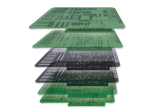
To figure out the over-current capability of the PCB, we first start with the PCB structure. Take a double-layer PCB as an example. This kind of circuit board usually has a three-layer structure: copper skin, plate, and copper skin. The copper skin is the path through which the current and signal in the PCB pass.

According to the knowledge of middle school physics, we can know that the resistance of an object is related to the material, cross-sectional area, and length. Since our current runs on the copper skin, the resistivity is fixed. The cross-sectional area can be regarded as the thickness of the copper skin, which is the copper thickness in the PCB processing options. Usually the copper thickness is expressed in OZ, the copper thickness of 1OZ is 35um, 2OZ is 70um, and so on. Then it can be easily concluded that when a large current is to be passed on the PCB, the wiring should be short and thick, and the thicker the copper thickness of the PCB, the better.
In actual PCB engineering, there is no strict standard for the length of wiring. Usually used in engineering: copper thickness / temperature rise / wire diameter, these three indicators to measure the current carrying capacity of the PCB board.
With a 1OZ copper-thick circuit board, at a temperature rise of 10°, a wire with a width of 100mil (2.5mm) can pass a current of 4.5A. And as the width increases, the current-carrying capacity of the PCB does not strictly increase linearly, but the increase gradually decreases, which is also consistent with the actual project. If the temperature rise is increased, the current carrying capacity of the wire can also be improved.
PCB wiring experience is: increasing the copper thickness, widening the wire diameter, and improving the heat dissipation of the PCB can enhance the current-carrying capacity of the PCB.
So if I want to run a current of 100 A, I can choose a copper thickness of 4 OZ, set the trace width to 15 mm, double-sided traces, and add a heat sink to reduce the temperature rise of the PCB and improve stability.
Method 2: Terminal
In addition to wiring on the PCB, wiring posts can also be used. Fix several terminals that can withstand 100A on the PCB or the product shell, such as surface mount nuts, PCB terminals, copper columns, etc. Then use terminals such as copper lugs to connect wires that can withstand 100A to the terminals. In this way, large currents can pass through the wires.
Method 3: Customized copper busbar
Even copper bars can be customized. It is a common practice in the industry to use copper bars to carry large currents. For example, transformers, server cabinets and other applications use copper bars to carry large currents.
Method 4: Special process
In addition, there are some special PCB processes, such as a 3-layer copper layer design, the top and bottom layers are signal wiring layers, and the middle layer is a copper layer with a thickness of 1.5mm, which is specially used to lay out the power supply. This kind of PCB board can be easily made. To a small volume of over current 100A.