1. How to reduce EMI problems by arranging stacks?
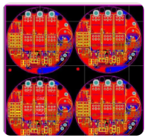
In PCB design, first of all, EMI must be considered from the system. PCB alone cannot solve the problem. In terms of EMI, I think the main purpose of stacking is to provide the shortest return path for the signal, reduce the coupling area, and suppress differential mode interference. In addition, the ground layer is tightly coupled with the power layer, which is more epitaxial than the power layer, which is good for suppressing common mode interference.
2. Why should copper be laid?
There are generally several reasons for copper paving. 1. EMC. For large-area ground or power supply copper, it will play a shielding role, and some special grounds, such as PGND, play a protective role. 2. PCB process requirements. Generally, in order to ensure the electroplating effect, or the lamination is not deformed, copper is laid on the PCB layer with less wiring. 3. The signal integrity requirements provide a complete return path for high-frequency digital signals and reduce the wiring of the DC network. Of course, there are also reasons such as heat dissipation, special device installation requires copper and so on.
3. In a system, dsp and pld are included. What problems should be paid attention to when wiring?
Look at the ratio of your signal rate to the length of the wiring. If the time delay of the signal in the transmission line is comparable to the time of the signal change edge, the signal integrity problem must be considered. In addition, for multiple DSPs, clocks, and data signal routing will also affect signal quality and timing, which requires attention.
4. In addition to the protel tool wiring, are there other good tools?
As for tools, in addition to PROTEL, there are many wiring tools, such as WG2000 from MENTOR, EN2000 series and powerpcb, allegro from Cadence, cadstar from Zuken, cr5000, etc., each with its own strengths.

5. What is the "signal return path"?
Signal return path, that is, return current. When high-speed digital signals are transmitted, the signal flows from the driver along the PCB board transmission line to the load, and then from the load back to the driver through the shortest path along the ground or power supply. This return signal on the ground or power supply is called the signal return path. Dr. Johson explained in his book that high-frequency signal transmission is actually a process of charging the dielectric capacitor sandwiched between the transmission line and the DC layer. SI analyzes the electromagnetic characteristics of the enclosure and the coupling between them.
6. How to perform SI analysis on connectors?
In the IBIS3.2 specification, there is a description of the connector model. The EBD model is generally used. If it is a special board, such as a backplane, a SPICE model is required. You can also use multi-board simulation software (HYPERLYNX or IS_multiboard). When building a multi-board system, enter the distribution parameters of the connectors, which are generally obtained from the connector manual. Of course, this method will not be accurate enough, but as long as it is within the acceptable range.
7. What are the termination methods?
Termination (terminal), also known as matching. Generally, it is divided into active end matching and terminal matching according to the matching position. Among them, the source terminal matching is generally resistance series matching, and the terminal matching is generally parallel matching. There are many ways, including resistance pull-up, resistance pull-down, Thevenin matching, AC matching, and Schottky diode matching.
8. What factors determine the way of termination (matching)?
The matching method is generally determined by the characteristics of the BUFFER, the topology, the type of level and the judgment method, and the signal duty cycle, system power consumption, etc. should also be considered.
9. What are the rules for using termination (matching)?
The most critical aspect of the digital circuit is the timing issue. The purpose of adding matching is to improve the signal quality and obtain a determinable signal at the moment of decision. For level-valid signals, the signal quality is stable under the premise of ensuring the setup and hold time; for the valid signals, the signal change delay speed meets the requirements under the premise of ensuring the monotonicity of the signal delay. Mentor ICX product textbooks have some information about matching. In addition, "High Speed Digital design a hand book of blackmagic" has a chapter dedicated to the terminal, which describes the effect of matching on signal integrity from the principle of electromagnetic waves, which can be used for reference.
10. Can the IBIS model of the device be used to simulate the logic function of the device in PCB layout and design? If not, how to perform board-level and system-level simulation of the circuit?
The IBIS model is a behavioral model and cannot be used for functional simulation. For functional simulation, SPICE models or other structural-level models are required.