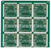
The ways to suppress interference on the PCB board are:
1. Reduce the area of the differential mode signal loop.
2. Reduce high frequency noise return (filtering, isolation and matching).
3. Reduce the common mode voltage (grounding design). 47 principles of high-speed PCB EMC design II. Summary of PCB design principles
Principle 1: PCB clock frequency exceeds 5MHZ or signal rise time is less than 5ns, generally need to use multi-layer board design.
Reason: The area of signal loop can be well controlled by adopting multi-layer board design.
Principle 2: For multilayer boards, the key wiring layer (the layer where the clock line, bus, interface signal line, radio frequency line, reset signal line, chip select signal line, and various control signal lines are located) should be adjacent to the complete ground plane. Preferably between two ground planes.
Reason: The key signal lines are generally strong radiation or extremely sensitive signal lines. Wiring close to the ground plane can reduce the signal loop area, reduce the radiation intensity or improve the anti-interference ability.
Principle 3: For single-layer boards, both sides of key signal lines should be covered with ground.
Reason: The key signal is covered with ground on both sides, on the one hand, it can reduce the area of the signal loop, and on the other hand, it can prevent the crosstalk between the signal line and other signal lines.
Principle 4: For a double-layer board, a large area of ground should be laid on the projection plane of the key signal line, or the same as a single-sided board.
Reason: the same as that the key signal of the multilayer board is close to the ground plane.
Principle 5: In a multilayer board, the power plane should be retracted by 5H-20H relative to its adjacent ground plane (H is the distance between the power supply and the ground plane).
Reason: The indentation of the power plane relative to its return ground plane can effectively suppress the edge radiation problem.
Principle 6: The projection plane of the wiring layer should be in the area of the reflow plane layer.
Reason: If the wiring layer is not in the projection area of the reflow plane layer, it will cause edge radiation problems and increase the signal loop area, resulting in increased differential mode radiation.
Principle 7: In the multilayer board, the TOP and BOTTOM layers of the single board should not have signal lines larger than 50MHZ as much as possible. Reason: It is best to walk the high-frequency signal between the two plane layers to suppress its radiation to the space.

Principle 8: For a single board with a board-level operating frequency greater than 50MHz, if the second layer and the penultimate layer are wiring layers, the TOP and BOOTTOM layers should be covered with grounded copper foil.
Reason: It is best to walk the high-frequency signal between the two plane layers to suppress its radiation to the space.
Principle 9: In a multilayer board, the main working power plane (the most widely used power plane) of the single board should be in close proximity to its ground plane.
Reason: The adjacent power plane and ground plane can effectively reduce the loop area of the power circuit.
Principle 10: In a single-layer board, there must be a ground wire next to and parallel to the power trace.
Reason: reduce the area of the power supply current loop.
Principle 11: In a double-layer board, there must be a ground wire next to and parallel to the power trace.
Reason: reduce the area of the power supply current loop.
Principle 12: In the layered design, try to avoid adjacent wiring layers. If it is unavoidable that the wiring layers are adjacent to each other, the layer spacing between the two wiring layers should be appropriately increased, and the layer spacing between the wiring layer and its signal circuit should be reduced.
Reason: Parallel signal traces on adjacent wiring layers can cause signal crosstalk.
Principle 13: Adjacent plane layers should avoid overlapping of their projection planes.
Reason: When the projections overlap, the coupling capacitance between the layers will cause the noise between the layers to couple with each other.
Principle 14: When designing the PCB layout, fully observe the design principle of placing in a straight line along the signal flow direction, and try to avoid looping back and forth.
Reason: Avoid direct signal coupling and affect signal quality.
Principle 15: When multiple module circuits are placed on the same PCB, digital circuits and analog circuits, and high-speed and low-speed circuits should be laid out separately.
Reason: Avoid mutual interference between digital circuits, analog circuits, high-speed circuits, and low-speed circuits.
Principle 16: When there are high, medium, and low-speed circuits on the circuit board at the same time, follow the high-speed and medium-speed circuits and stay away from the interface.
Reason: Avoid high-frequency circuit noise from radiating to the outside through the interface.
Principle 17: Energy storage and high-frequency filter capacitors should be placed near unit circuits or devices with large current changes (such as power supply modules: input and output terminals, fans and relays).
Reason: The existence of energy storage capacitors can reduce the loop area of large current loops.
Principle 18: The filter circuit of the power input port of the circuit board should be placed close to the interface. Reason: to prevent the line that has been filtered from being coupled again.
Principle 19: On the PCB circuit board, the filtering, protection and isolation components of the interface circuit should be placed close to the interface.
Reason: It can effectively achieve the effects of protection, filtering and isolation.
Principle 20: If there is both a filter and a protection circuit at the interface, the principle of first protection and then filtering should be followed.
Reason: The protection circuit is used for external overvoltage and overcurrent suppression. If the protection circuit is placed after the filter circuit, the filter circuit will be damaged by overvoltage and overcurrent.