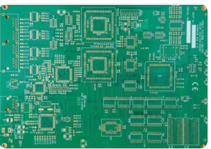
If there are no vias, the PCB will not work. Vias are conduits that transmit signals between PCB layers. During PCB production, PCB manufacturers add a layer of copper on the substrate. This layer of copper not only makes the traces conductive, but also connects each PCB layer through holes drilled into the board. Then, the manufacturer can leave the via as it is and use the copper plating to transmit the signal on its own. However, in order to increase the capacity, it is also possible to fill the via with another conductive material.
To make copper-filled vias, the manufacturer fills the vias with epoxy and copper. The additional materials increase the cost of circuit board production, but copper-filled vias make PCBs more suitable for certain applications. Copper-filled vias also have functions that other conductive fillers cannot provide. The following will introduce the main uses of copper-filled vias and how they can enhance PCB design.
1. Through hole filling process
When filling the via with copper, the manufacturer must take care to form a uniform copper layer in the via without creating a too thick outer layer. If the technology used is not correct, too much copper will be produced, thereby increasing the weight of the PCB or adding too much copper, resulting in non-compliance with specifications, defects or increased costs. As through holes become smaller than ever, observing these requirements is critical to meeting stringent design specifications.
The classic copper via filling method involves filling the hole with pure copper. However, this method often creates voids, allowing contaminants to be trapped in the copper. When heated in future production steps, this void will release gas, creating holes that break the connections between the copper layers of the PCB. Current strategies to prevent this problem include leaving grooves in the filled vias and forming "X" pattern connections in the vias.
2. The benefits of copper filled vias
A PCB with copper-filled vias has the following advantages compared to a circuit board with only copper-plated vias:
Thermal conductivity: Filling the via with copper can improve its thermal conductivity.
In applications involving high temperatures, keeping heat away from the circuit board can extend its life and prevent defects.
The high thermal conductivity of copper attracts this heat and keeps it away from critical areas of the PCB.
Conductivity: Copper-filled vias are also suitable for applications that require strong current to be conducted from one side of the circuit board to the other.
The conductivity of copper allows large currents to pass through deeper layers without overloading the PCB.
Because of this ability, designers often require copper-filled vias on the PCB, which can withstand higher voltages.
3. Application of filled vias and electroplated vias

Although PCBs with copper-filled vias increase the capacity, they are also more expensive to produce than PCBs with plated vias. In some cases, it is also necessary to improve the reliability associated with copper-filled vias. However, some applications can also apply copper-plated vias next to the copper traces.
When you decide on the PCB vias, you must consider the heat and voltage intensity involved in the application. In low-stress applications, qualified PCBs with plated vias can work flawlessly. At the same time, PCBs with copper-filled vias can withstand the conditions required for high power, radio frequency, microwave, and LED applications. High-power integrated circuits running these types of PCBs need to use copper filled vias instead of plated vias to withstand the current.
4. Copper, silver conductive epoxy resin and gold filled vias
In addition to filling PCB vias with copper, PCB factories can also choose to use silver conductive epoxy. However, although silver conductive epoxy seems to be a good choice, it is more costly and not as efficient as copper. In addition, you can also choose to use gold-plated vias, but compared with gold, copper has the following advantages:
Higher thermal conductivity
Higher conductivity
More cost-effective price
Longer life
more reliable
Better capacity for high-power applications
Even at a lower price, copper-filled vias are still better than gold-plated vias. Their higher thermal and electrical conductivity enable them to conduct excess heat more efficiently. Copper vias can also handle higher voltages without overloading.