PCB engineering design requirements
According to the conventional solder mask engineering design, the size of the single-sided solder mask is required to be greater than the size of the flux pad by 0.05mm, otherwise there will be a risk of the solder mask covering the flux layer. As shown in Figure 5 above, the width of one-sided solder mask is 0.05mm, which meets the requirements of solder mask production and processing. However, the edge distance between the two resist pads is only 0.05mm, which does not meet the minimum solder resist bridge process requirements. The engineering design directly designs the entire row of pins of the chip as a group-pad type window design. As shown in Figure 6:
What impact will the unreasonable PCB soldering design have on the PCBA manufacturing process?
What are the consequences of unreasonable PCB soldering design
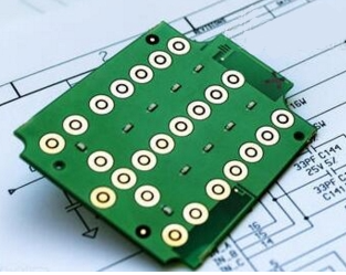
Actual welding effect
After making the board according to the engineering design requirements, and completing the SMT patch. It is verified by functional tests that the chip has a defective soldering rate of more than 50%; after passing the temperature cycle experiment again, a defective rate of more than 5% can be screened out. Firstly, perform appearance analysis of the device (20 times magnifying glass), and find that there are tin slag and residues after soldering between the adjacent pins of the chip; secondly, analyze the failed products and find that the failed chip pins are short-circuited and burned.
What impact will the unreasonable PCB soldering design have on the PCBA manufacturing process?
Optimization
Research on PCB Solder Mask Design and PCBA Manufacturability
PCB LAYOUT design optimization

Refer to the IPC 7351 standard package library, the solder pad design is 1.2mm*0.3mm, the solder mask design is 1.3*0.4mm, and the center spacing between adjacent pads remains unchanged at 0.65mm. Through the above design, the size of single-sided solder mask of 0.05mm meets the requirements of PCB processing technology, and the size of adjacent solder mask edges of 0.25mm meets the process of solder mask bridge. Increasing the redundant design of solder mask bridge can greatly reduce the welding quality risk., Thereby improving the reliability of the product.
What impact will the unreasonable PCB soldering design have on the PCBA manufacturing process?
PCB engineering design optimization
The width of the soldering pad is cut copper, and the size of the solder mask width is adjusted. Ensure that the distance between the edges of the two soldering pads of the device is greater than 0.2mm, and the distance between the edges of the two soldering resist pads is greater than 0.1mm, and the lengths of the soldering pads and soldering resist pads remain unchanged. Meet the manufacturability requirements of PCB solder mask single-pad type window design.
What impact will the unreasonable PCB soldering design have on the PCBA manufacturing process?
Demonstration program
Research on PCB Solder Mask Design and PCBA Manufacturability
Design verification
In view of the above-mentioned problem pads, the pads and solder mask design are optimized through the above solutions. The edge spacing of adjacent pads is greater than 0.2mm, and the edge spacing of solder mask pads is greater than 0.1mm. This size can meet the solder mask process. need.
What impact will the unreasonable PCB soldering design have on the PCBA manufacturing process?
Test yield comparison
After optimizing the solder mask design from the PCB LAYOUT design and PCB engineering design, the organization re-invested the same number of PCBs and completed the placement and production according to the same manufacturing process.
What impact will the unreasonable PCB soldering design have on the PCBA manufacturing process?
Through the above data, the optimization scheme is verified to be effective and meets the product manufacturability design.
Optimized design summary
Research on PCB Solder Mask Design and PCBA Manufacturability
To sum up, the chip with the device pin edge spacing less than 0.2mm cannot be designed according to the conventional packaging. The width of the soldering pad in the PCB LAYOUT design is not compensated, and the length of the soldering pad is increased to avoid the reliability problem of the soldering contact area. If the soldering pad is too large and the distance between the two solder mask edges is too small, priority should be given to copper removal; for the solder mask that is too large, the solder mask design should be optimized to effectively increase the edge width of the two solder masks to ensure PCBA Welding quality assurance. It can be seen that the coordination between soldering flux and solder mask pad design plays a decisive role in improving PCBA manufacturability and soldering through rate.