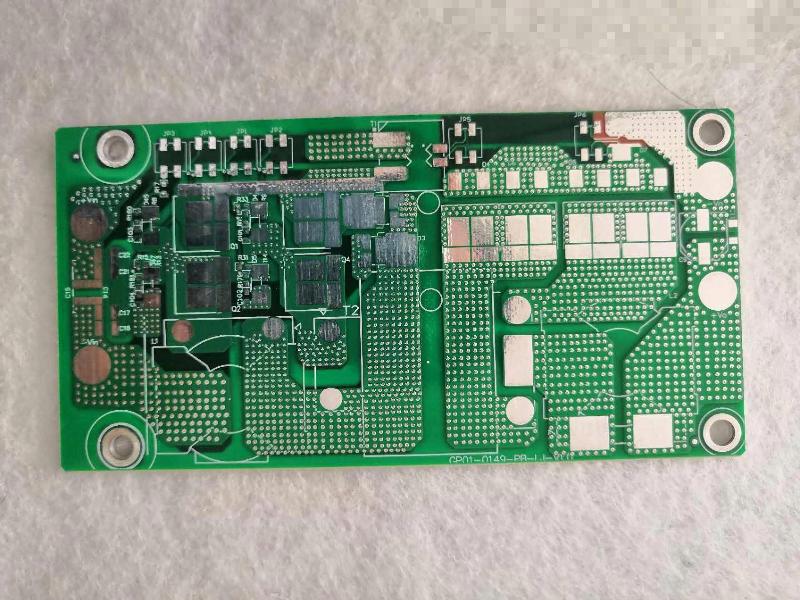
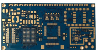
With the rapid development of modern electronic technology, PCBA is also developing towards high density and high reliability. Although the level of PCB and PCBA manufacturing processes has been greatly improved at this stage, conventional PCB solder mask processes will not have a fatal impact on product manufacturability. But for devices with very small device pin spacing, due to the unreasonable PCB solder pad design and PCB solder mask design, it will increase the difficulty of the SMT soldering process and increase the risk of PCBA surface mount processing quality. In view of the manufacturability and reliability problems caused by the unreasonable PCB soldering and solder mask design, combined with the actual process level of PCB and PCBA, the manufacturability problem can be avoided by optimizing the design of the device package. The optimization design mainly starts from two aspects. One is the optimization design of PCB LAYOUT; the second is the optimization design of PCB engineering.
PCB solder mask design status
Research on PCB Solder Mask Design and PCBA Manufacturability
PCB LAYOUT design
According to the IPC 7351 standard package library and refer to the recommended pad size of the device specification for package design. In order to design quickly, Layout engineers give priority to increase and modify the design according to the recommended pad size. The PCB solder pad design length and width are increased by 0.1mm, and the solder mask pad is also different in length and width based on the solder pad size. Increase by 0.1mm.
What are the consequences of unreasonable PCB soldering design
What impact will the unreasonable PCB soldering design have on the PCBA manufacturing process?

PCB engineering design
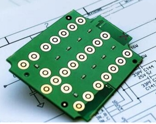
The conventional PCB solder mask process requires to cover the edge of the solder pad by 0.05mm, and the middle solder mask bridge between the two solder pads is greater than 0.1mm. In the PCB engineering design stage, when the size of the solder mask cannot be optimized, the two The solder resist bridge between the pads is less than 0.1mm, and the PCB project adopts the group pad window design process.
What are the consequences of unreasonable PCB soldering design
What impact will the unreasonable PCB soldering design have on the PCBA manufacturing process?
PCB solder mask design requirements
Research on PCB Solder Mask Design and PCBA Manufacturability
PCB LAYOUT design requirements
When the edge distance between two soldering pads is greater than 0.2mm, the package is designed according to the conventional pad; when the edge distance between the two soldering pads is less than 0.2mm, DFM optimization design is required, DFM The optimization design method includes the optimization of soldering flux and solder mask pad size. Ensure that the solder mask in the solder mask process can form the smallest solder mask bridge isolation pad during PCB manufacturing.
What are the consequences of unreasonable PCB soldering design
What impact will the unreasonable PCB soldering design have on the PCBA manufacturing process?
PCB engineering design requirements
When the edge distance between the two soldering pads is greater than 0.2mm or more, engineering design shall be carried out according to the conventional requirements; when the edge distance between the two soldering pads is less than 0.2mm, DFM design is required. The engineering design DFM method has solder mask design optimization And the soldering layer copper removal treatment; the copper removal size must refer to the device specification, the soldering soldering layer pad after copper removal should be within the size range of the recommended pad design, and the PCB solder mask design should be a single-pad window design, That is, the solder mask bridge can be covered between the pads. Ensure that in the PCBA manufacturing process, there is a solder mask bridge between the two pads for isolation to avoid solder appearance quality problems and electrical performance reliability problems.
PCBA process capability requirements
Research on PCB Solder Mask Design and PCBA Manufacturability
The solder mask can effectively prevent the solder bridge from shorting during the soldering assembly process. For PCBs with high-density and fine-pitch pins, if there is no solder mask bridge between the pins for isolation, the PCBA processing plant cannot guarantee the local soldering quality of the product. For PCBs with high-density and fine-pitch pins without solder mask isolation, the current PCBA manufacturing plant's processing method is to determine that the PCB incoming materials are bad and will not be put into production. If the customer insists on going online, the PCBA manufacturing factory will not guarantee the welding quality of the product in order to avoid quality risks. It is predicted that the welding quality problems that occur during the manufacturing process of the PCBA factory will be negotiated and dealt with.
case analysis
Research on PCB Solder Mask Design and PCBA Manufacturability
Device specification size
Device pin center spacing: 0.65mm, pin width: 0.2~0.4mm, pin length: 0.3~0.5mm.
What are the consequences of unreasonable PCB soldering design
What impact will the unreasonable PCB soldering design have on the PCBA manufacturing process?
PCB LAYOUT actual design
The size of the soldering pad is 0.8*0.5mm, the size of the solder mask is 0.9*0.6mm, the center spacing of the device pads is 0.65mm, the spacing of the soldering edges is 0.15mm, and the spacing of the soldering masks is 0.05mm., The width of single-side solder mask is increased by 0.05mm.
What are the consequences of unreasonable PCB soldering design
What impact will the unreasonable PCB soldering design have on the PCBA manufacturing process?