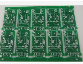
The multi-layer PCB is composed of conductive materials. It includes the plane between the PCB and the additional PCB signal layer. For example, a typical six-layer PCB printed circuit board consists of two inner layers, two outer layers and two inner layers, one for the PCB power supply and one for the ground. Such a design can improve electromagnetic interference and provide better routing options for low-speed and high-speed signals. A two-layer surface layer helps low-speed signal transmission, while two inner layers help high-speed signals.
Six-layer PCB
The correct stacking of 6-layer PCB can make its performance more perfect. Due to the use of different types of radio frequency equipment, it can effectively suppress EMI and contains multiple spacing components. Any error in the design will affect the perfect performance of the PCB. So how should we design to give full play to the perfect performance of PCB?
First of all, before designing, we need to analyze and solve the number of grounding, power and signal planes that the PCB may need. Bonding layers are an important part of any laminate because they provide better shielding for the laminate, and they reduce the need for external shielding cans.
If you want to plan a dense circuit board with a small footprint for wiring, you can install four signal layers, a ground layer, and a power layer. In the high-density circuit board, a mixture of wireless signals and analog signals is used. The superposition method of signal layer/ground/power layer/ground/signal layer/ground layer separates the inner and outer signal layers, which has both internal and external signals. Floor. This layered design helps suppress the mixing of EMI in the internal signal layer. Stacked designs are also ideal for RF equipment, because AC power and ground planes provide excellent decoupling.
Dense PCB circuit board

If you want to build a printed circuit board with many sensitive circuits, it is best to choose a stack like this: signal/power/2 signal/ground/signal, which can protect sensitive traces well and is more suitable for high-frequency analog signals Or high-speed digital signal circuit. These signals will be separated from the low-speed signals in the outer layer. This shielding is done on the inner layer, which also allows signal routing of different frequencies or switching speeds.
A printed circuit board
The stack of ground/signal layer/power/ground/signal layer/ground can be perfectly deployed on the circuit board near the strong radiation source. This stacking can effectively suppress electromagnetic interference and is also suitable for circuit boards used in noisy environments.
Since their six-layer PCB design has become a common feature of some advanced electronic circuits and is popular among electronic manufacturers, what are its specific advantages?
Six-layer PCB design
Due to their multi-layer design, they are relatively small compared to other circuit boards, which is particularly advantageous for miniature devices. The design of 6-layer PCB stacking requires a lot of planning, which can reduce errors in details and ensure high-quality construction. Currently, different testing and inspection techniques are generally used to ensure the applicability of the circuit board.
The compact printed circuit board is achieved by using lightweight components, which helps to reduce the overall weight of the printed circuit board. Unlike single-layer or double-layer PCBs, six-layer PCBs can interconnect components without multiple PCB connectors.
The 6-layer circuit board is composed of multiple insulating layers, which are made by bonding protective materials and different prepregs. This helps to improve the durability of these PCBs.
The 6-layer printed PCB has excellent electrical performance and compact design, which can effectively ensure high speed and high capacity.