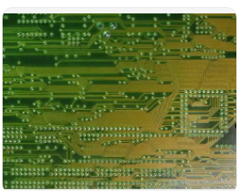
Before understanding the PCB circuit board design process, you must first understand what a PCB is the abbreviation of English Printed Circuit Board . Generally, conductive patterns made of printed circuits, printed components, or a combination of both on insulating materials according to a predetermined design are called printed circuits.
PCB was born in 1936, and the United States used this technology extensively in military radios in 1943; PCB technology has been widely adopted since the mid-1950s. At present, PCB has become the "mother of electronic products", and its applications have penetrated almost all terminal fields of the electronics industry, including computers, communications, consumer electronics, industrial control, medical instruments, national defense, military industry, aerospace and many other fields. The following is a detailed explanation of the PCB design process compiled by the Fast PCB Academy.
1. Preliminary preparation
Including the preparation of component libraries and schematic diagrams. Before proceeding with PCB design, we must first prepare the schematic SCH component library and PCB component packaging library.

The PCB component package library is best established by the engineer based on the standard size data of the selected device. In principle, establish the PC component package library first, and then establish the schematic SCH component library.
PCB component package library requirements are high, which directly affects the installation of PCB; schematic diagram SCH component library requirements are relatively loose, but pay attention to define the pin attributes and the corresponding relationship with the PCB component package library.
2. PCB structure design
According to the determined circuit board size and various mechanical positioning, draw the PCB frame in the PCB design environment, and place the required connectors, buttons/switches, screw holes, assembly holes, etc. according to the positioning requirements.
Fully consider and determine the wiring area and non-wiring area (such as how much area around the screw hole belongs to the non-wiring area).
3. PCB layout design
The layout design is to place the components in the PCB frame according to the design requirements. Generate the netlist (Design-Create Netlist) in the schematic tool, and then import the netlist (Design-Import Netlist) in the PCB software. After the netlist is successfully imported, it will exist in the background of the software. Through the Placement operation, all devices can be called out, and there is a flying line prompt connection between the pins. At this time, the layout design of the device can be carried out.
PCB layout design is the first important process in the entire PCB design process. The more complex the PCB board, the better the layout can directly affect the difficulty of later wiring.
Layout design depends on the circuit board designer's basic circuit knowledge and rich design experience, which is a higher level requirement for the circuit board designer. Elementary circuit board designers have little experience and are suitable for small module layout design or PCB layout design tasks with lower overall board difficulty.
4. PCB wiring design
PCB layout design is the process with the largest workload in the entire PCB design, which directly affects the performance of the PCB board.
In the PCB design process, wiring generally has three realms:
The first is the distribution, which is the most basic entry requirement for PCB design;
The second is the satisfaction of electrical performance, which is a standard to measure whether a PCB board is qualified. After the wiring is laid out, carefully adjust the wiring to achieve the best electrical performance;
Thirdly, neat and beautiful, chaotic wiring, even if the electrical performance is passed, it will cause great inconvenience to the later modification of the board optimization and testing and maintenance. The wiring requirements are neat and uniform, and they cannot be crisscrossed and disordered.
5. Wiring optimization and silk screen placement
"PCB design is not the best, only better", "PCB design is an art of defects", this is mainly because PCB design needs to realize the design requirements of all aspects of hardware, and individual requirements may be in conflict with each other. Bear's paw can't have both.
For example: a PCB design project needs to be designed as a 6-layer board after evaluation by the circuit board designer, but the product hardware must be designed as a 4-layer board due to cost considerations, so the signal shielding ground layer can only be sacrificed, resulting in adjacent wiring The signal crosstalk between layers increases and the signal quality decreases.
The general design experience is: the time to optimize the wiring is twice the time of the first wiring. After the PCB layout optimization is completed, post-processing is required. The first thing to do is the silk screen logo on the PCB surface. The bottom silk screen characters need to be mirrored during the design to avoid confusion with the top silk screen.
6. Network DRC inspection and structure inspection
Quality control is an important part of the PCB design process. General quality control methods include: design self-inspection, design mutual inspection, expert review meetings, special inspections, etc.
Schematic diagram and structural element diagram are the most basic design requirements. Network DRC inspection and structural inspection are to confirm that the PCB design meets the two input conditions of the schematic netlist and structural element diagram.
Generally, circuit board designers will have their own accumulated design quality check Checklist, where the entries partly come from the company or department's specifications, and the other part comes from their own experience summaries. Special inspections include Valor inspection and DFM inspection of the design. These two parts focus on the PCB design and output back-end processing gerber files.
7. PCB system board
Before the PCB is formally processed and manufactured, the circuit board designer needs to communicate with the PE of the PCB supplier to answer the manufacturer's confirmation questions about the PCB board processing.
This includes but is not limited to: selection of PCB board model, adjustment of circuit layer line width and line spacing, adjustment of impedance control, adjustment of PCB stacking thickness, surface treatment processing technology, aperture tolerance control and delivery standards, etc.