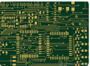
1. Visual inspection
Since the various layers in the PCB are tightly integrated, it is generally not easy to see the actual number, but if you carefully observe the board card fault, you can still distinguish it. Careful, we will find that there is one or several layers of white material between the PCB. In fact, this is the insulating layer between the layers to ensure that there will be no short circuit between different PCB layers. Because the current multi-layer PCB boards use more single or double-sided wiring boards, and a layer of insulating layer is placed between each layer and pressed together, the number of layers of the PCB board means that there are several independent layers. The wiring layer, and the insulating layer between layers has become the most intuitive way for us to judge the number of PCB layers.
How to see the number of PCB layers
2. Guide hole and blind hole alignment method
The guide hole method uses the "guide hole" on the PCB to identify the number of PCB layers. The principle is mainly due to the via technology used in the circuit connection of the multilayer PCB. If we want to see how many layers the PCB has, we can distinguish by observing the via holes.
On the most basic PCB (single-sided motherboard), the parts are concentrated on one side, and the wires are concentrated on the other side. If you want to use a multi-layer board, you need to punch holes on the board so that the component pins can pass through the board to the other side, so the guide holes will penetrate the PCB board. So we can see that the pins of the part are soldered on the other side.
For example, if the board uses a 4-layer board, you need to route wires on the first and fourth layers (signal layer), and the other layers have other uses (ground layer and power layer). Place the signal layer on the power layer and The purpose of the two sides of the ground layer is to prevent mutual interference and facilitate correction of the signal line. If some board card guide holes appear on the front side of the PCB board but cannot be found on the back side, then it must be a 6/8-layer board. If the same via holes can be found on both sides of the PCB, it will naturally be a 4-layer board.

However, many board card manufacturers currently use another routing method, which is to connect only some of the lines, and uses buried vias and blind vias in the routing. Blind vias are to connect several layers of internal PCB to the surface PCB without penetrating the entire circuit board.
Buried vias only connect the internal PCB, so they are not visible from the surface. Since the blind hole does not need to penetrate the entire PCB, if it is six layers or more, look at the board facing the light source, the light will not pass through. So there was a very popular saying before: judging four-layer and six-layer or above PCBs by whether the vias leak light. This method has its reasons, and it is not applicable, so it can be used as a reference method.
3. Accumulation method
To be precise, this is not a method, but an experience. But this is what we think is the most accurate. We can judge the number of layers of the PCB through the traces of some public PCB boards and the position of the components. Because in the current IT hardware industry that is changing so quickly, there are not many PCB manufacturers capable of redesigning PCBs.
For example, a few years ago, a large number of 9550 graphics cards designed with 6-layer PCB were used. If you are careful, you can compare how much it is different from 9600PRO or 9600XT. Just omit some components, and maintain the same height on the PCB.
In the 1990s of the last century, there was a widespread saying at that time: the number of PCB layers can be seen by placing the PCB upright, and many people believed it. This statement was later proved to be nonsense. Even if the manufacturing process at the time was backward, how could the eye be able to tell it at a distance smaller than the hair? Later, this method continued and modified, and gradually evolved another measurement method. Nowadays, many people believe that it is possible to measure the number of PCB layers with precision measuring instruments such as "vernier calipers", and we do not agree with this statement.
Regardless of whether there is that kind of precision instrument, why don't we see that a 12-layer PCB is 3 times the thickness of a 4-layer PCB? Different PCBs will use different manufacturing processes. There is no uniform standard for measurement. How to judge the number of layers based on the thickness?
In fact, the number of PCB layers has a great influence on the board. For example, why at least 6 layers of PCB should be used to install dual CPU? Because of this, the PCB can have 3 or 4 signal layers, 1 ground layer, and 1 or 2 power layers. Then the signal lines can be separated far enough to reduce mutual interference, and there is enough current supply. However, a 4-layer PCB design for general boards is completely sufficient, while a 6-layer PCB is too costly and does not have most performance improvements.