Antenna is an important part of all kinds of intelligent devices, and all devices that need to use wireless need to use it. Now is the era of wireless, network routers are wireless WiFi, computers, mobile phones, even the network no longer need to connect the network cable, there are Bluetooth headset, Bluetooth mouse, Bluetooth keyboard and so on. The performance of this antenna is very important.
In general, there are some factors in the selection of antenna. In addition to considering the performance, but also considering the cost, when choosing the antenna, we need to consider comprehensively. Today, ipcb will tell you about various antenna PCB design and design points.

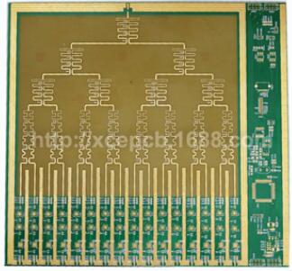
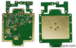
Antenna PCB
PCB antennas generally have the following types,
The first PCB antenna
This kind of antenna is low cost, but its performance is slightly worse. There are also several forms of PCB antenna.
a. Planar inverted-F antenna, abbreviated as PIFA,
What problems should be paid attention to in the PCB design of this inverted-F antenna?
First of all, we need to know the knowledge of RF PCB. For RF PCB, any copper foil, wire can not be regarded as a simple wire. It is an equivalent circuit composed of many resistance capacitance circuits. If you see a short circuit, it is not a short circuit for the RF PCB. In this way, let's take a look at the PCB design of the inverted-F antenna.
This PCB antenna has six points to pay attention to:
1. This inverted F antenna is not drawn casually. There is a special library of this antenna. Take it and put it on as required. If the space is not enough, it is that they have made their own special antenna through simulation.
2. The line impedance from RF feed point must be 50ohm.
3. The grounding feed point must be grounded firmly.
4. More holes must be drilled on the ground plane,
5. All layers of copper foil for PCB antenna must be clear.
6. The antenna must be placed in the corner of PCB board, and the three sides should be empty.
The antenna on the mobile phone is called planar inverted-F antenna. In principle, it is composed of a plane connected with a grounding plane feed point and RF feed point. However, the antenna in the mobile phone adopts a planar structure. The performance of this inverted-F antenna is much better than that of PCB antenna, which has less space and lower cost. It is the best choice for mobile phone antenna.
In fact, this plane has many shapes for different mobile phones. The principle is planar inverted-F structure. In this plane, one is connected to RF and the other is grounded. The planar inverted-F antenna is formed.
b. Inverted L-shaped PCB antenna
The problems needing attention of this inverted-L antenna are almost the same as the previous ones. The effect of inverted L-shaped antenna is better than that of inverted-F antenna, because the inverted-F antenna has a grounding feed point, which can effectively adjust the frequency point.
There are many PCB antennas on the market, some of which are made by PCB antenna manufacturers themselves through simulation.
The second kind of ceramic PCB antenna
This kind of antenna is made into a chip element. One end of the antenna is connected with RF and the other end is grounded. The principle of ceramic antenna is to change the high-frequency electric field between the antenna and the ground into electromagnetic wave through an electrode called "antenna", which can be transmitted and transmitted to the distance.
The best layout and routing of PCB is as follows
When the ceramic patch antenna is placed on the board, the antenna is grounded while the RF signal is connected. All layers of copper foil below are hollowed out (the area shown in the white box). At least two directions are empty in such four directions, which is very good for the antenna. Don't forget that the grounding copper foil should be drilled with grounding through holes, and more holes should be drilled.
The third kind of rod antenna
This kind of antenna has the best effect. It is placed in the space and has the best radiation effect. However, the cost is a little more expensive and the space occupied is also large, which can only be exposed outside the shell.
Some problems should be paid attention to in PCB design
1. If the RF lead wire is short, all layers under the RF signal line should have clearance. If the outgoing line is long, the impedance of this outlet should be controlled. If the multi-layer board is used, the clearance of the second layer under the RF signal line should be covered with complete copper, and then the impedance of the interlayer reference ground should be controlled at 50ohm
2. The nearby grounding copper foil must be grounded firmly, that is to say, more ground holes should be drilled.