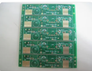
As a PCB design engineer, everyone knows that the impedance must be continuous. However, as Luo Yonghao said, "There are always times when I step on my stool in my life", there are always times when the impedance cannot be continuous in PCB design. What should I do at this time?
About impedance
Let's clarify a few concepts first. We often see impedance, characteristic impedance, and instantaneous impedance. Strictly speaking, they are different, but they are always the same. They are still the basic definition of impedance:
A) The input impedance at the beginning of the transmission line is referred to as impedance for short;
B) The instantaneous impedance encountered by the signal at any time is called the instantaneous impedance;
C) If the transmission line has a constant instantaneous impedance, it is called the characteristic impedance of the transmission line.

Characteristic impedance describes the transient impedance experienced by the signal as it propagates along the transmission line. This is a major factor affecting the integrity of the signal in the transmission line circuit.
If there is no special instructions, the characteristic impedance is generally used to collectively refer to the transmission line impedance. The factors that affect the characteristic impedance are: dielectric constant, dielectric thickness, line width, and copper foil thickness.
The impedance is continuously similar:
The water flows steadily in a uniform ditch, and suddenly the ditch turns and widens.
Then the water will sway at the corners, and water waves will propagate.
This is the result of impedance mismatch.
The method to solve the impedance discontinuity
1, corner
If the RF signal line goes at a right angle, the effective line width at the corner will increase, and the impedance will be discontinuous, causing signal reflection. In order to reduce the discontinuity, to deal with the corners, there are two methods: chamfering and rounding. The radius of the arc angle should be large enough, generally speaking, to ensure: R>3W.
2, large pad
When there are large pads on the 50-ohm microstrip line, the large pads are equivalent to distributed capacitance, which destroys the continuity of the characteristic impedance of the microstrip line. Two methods can be taken to improve at the same time: firstly, thickening the microstrip line dielectric, and secondly, hollowing out the ground plane under the pad, which can reduce the distributed capacitance of the pad.
3, PCB via
Vias are one of the important factors that cause impedance discontinuities on the RF channel. The diameter, pad diameter, depth, and anti-pad of the vias will all bring changes, causing impedance discontinuities, reflections and the severity of insertion loss. . If the signal frequency is greater than 1GHz, the influence of vias must be considered.
Commonly used methods to reduce the discontinuity of via impedance are: adopting a diskless process, selecting an outlet method, optimizing the diameter of the anti-pad, and so on. Optimizing the anti-pad diameter is one of the most commonly used methods to reduce impedance discontinuities.
4, PCB through-hole coaxial connector
Similar to the PCB via structure, the PCB via coaxial connector also has impedance discontinuity, so the solution is the same as the via. Commonly used methods to reduce the impedance discontinuity of through-hole coaxial connectors are also: adopting a diskless process, a suitable outlet method, and optimizing the diameter of the anti-pad.