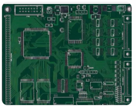
4 kinds of surface treatments for PCB circuit board proofing
The surface treatment methods used by PCB factories in circuit board proofing are different. Each surface treatment method has its own unique characteristics. Taking chemical silver as an example, its process is extremely simple. It is recommended to use lead-free soldering and smt, especially for The fine circuit effect is better. The most important thing is to use chemical silver for surface treatment, which will greatly reduce the overall cost and lower cost. Today we will introduce several common surface treatment methods for PCB proofing.
1. HASL hot air leveling (that is, spray tin)
Tin spraying is a common processing method in the early days of PCB proofing. It is now divided into lead spray tin and lead-free tin spray. The advantages of tin spraying: After the PCB is completed, the copper surface is completely wetted (the tin is completely covered before soldering), suitable for lead-free soldering, the process is mature and the cost is low, suitable for visual inspection and electrical testing, and it is also a high-quality and reliable PCB board One of the proofing processing methods.

2. Chemical nickel gold
Nickel gold is a relatively large-scale PCB proofing surface treatment process. Remember: the nickel layer is a nickel-phosphorus alloy layer. According to the phosphorus content, it is divided into high-phosphorus nickel and medium-phosphorus nickel. The application is different, so we will not introduce it here. the difference. The advantages of nickel gold: suitable for lead-free soldering; very flat surface, suitable for SMT, suitable for electrical testing, suitable for switch contact design, suitable for aluminum wire binding, suitable for thick plates, and strong resistance to environmental attacks.
3. Electroplating nickel gold
Electroplated nickel gold is divided into "hard gold" and "soft gold". Hard gold (such as gold-cobalt alloy) is commonly used on gold fingers (contact connection design), and soft gold is pure gold. Electroplating of nickel and gold is widely used on IC substrates (such as PBGA). It is mainly used for bonding gold and copper wires, but the IC substrate is suitable for electroplating. The bonding gold finger area requires additional conductive wires to be electroplated. The advantage of electroplating nickel-gold PCB board proofing is that it is suitable for contact switch design and gold wire binding, and is suitable for electrical testing.
4. Nickel Palladium
Nickel, palladium, gold is now gradually beginning to be used in the field of PCB proofing, and it has been used more in semiconductors before. Suitable for bonding of gold and aluminum wires. The advantage of proofing with nickel-palladium-gold PCB board is that it is applied on IC carrier board, suitable for gold wire bonding, aluminum wire bonding, and suitable for lead-free soldering. Compared with ENIG, there is no nickel corrosion (black plate) problem, and the cost is cheaper than ENIG and electro-nickel gold, suitable for a variety of surface treatment processes and on-board.