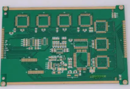
PCB circuit boards are widely used in China. Pollutants will be generated during the manufacturing process of printed PCB circuit boards, including flux and adhesive residues and other pollutants in the manufacturing process such as dust and debris. If the PCB board cannot effectively guarantee the clean surface, Resistance and leakage will cause the failure of the PCB circuit board, thereby affecting the service life of the product. Therefore, cleaning the PCB circuit board in the manufacturing process is an important step.
Semi-aqueous cleaning mainly uses organic solvents and deionized water, plus a certain amount of active agent, a cleaning agent composed of additives. This cleaning is between solvent cleaning and water cleaning. These cleaning agents are organic solvents, flammable solvents, PCBs The factory has a high flash point, low toxicity, and is safe to use, but it must be washed with water and then dried.

Water purification technology is the development direction of clean technology in the future. It is necessary to establish pure water source and discharge water treatment workshops. Using water as the cleaning medium, surfactants, additives, corrosion inhibitors and chelating agents are added to the water to form a series of Water-based cleaning agent can remove water solvents and non-polar contaminants.
Used in the PCB soldering process without clean flux or clean solder paste, directly enter the next process for cleaning after soldering, no longer free cleaning technology is currently the most commonly used alternative technology, especially mobile communication products are basically disposable The method used instead of OPCBADS. Solvent cleaning is mainly used to dissolve and remove contaminants. Solvent cleaning requires simple equipment due to its fast volatilization and strong solubility.
The above four cleaning technologies can achieve a certain cleaning effect, but how to clean the PCB board quickly and effectively? The application of the ultrasonic cleaning machine can be solved. It uses the role of UHF to transform into kinetic energy in the liquid medium to produce cavitation The effect is to form countless tiny bubbles, and then hit the surface of the object, so that the surface dirt will fall off, so as to achieve the cleaning effect, because it is through the liquid, as long as the liquid can touch the surface of the surface, it can be cleaned in place, leaving no dead corners. PCB circuit plate.
The cutting of PCB board, especially the cutting of multi-layer PCB board, is a time-consuming and laborious work, which contains a lot of repetitive labor. The designer must have enough patience and care, otherwise it is very easy to make mistakes. The key to a good cut PCB design is to use appropriate software to replace manual repetitive work, which saves time and is accurate.
A scanner must be used during the cutting process.
Many PCB designers are accustomed to drawing lines directly on PCB design systems such as PROTEL, PADSOR or CAD. This habit is very bad. The scanned graphics files are not only the basis for conversion into PCB document chip factory parts, but also the basis for later inspections., The use of a scanner can greatly reduce the labor difficulty and intensity. It is no exaggeration to say that if the scanner can be fully utilized, even people with no design experience can complete the PCB board cutting work.
In order to pursue speed, some designers choose two-way grinding plate (that is, grinding away the plate layer from the front and back surfaces to the middle layer). In fact, this is very wrong, because the two-way grinding plate is very easy to wear and cause other layers to be damaged. The result can be imagined. It is known that the outer layer of the PCB board is hard due to the process, copper foil, pads, etc., and the middle layer is soft. Therefore, the problem is more serious when it comes to the middle layer, and it often cannot be polished.