The role of the solder mask in controlling solder defects during the reflow soldering process is important, and the PCB designer should minimize the spacing or air gaps around the pad features.
Although many process engineers would rather separate all pad features on the board with a solder mask, the pin spacing and pad size of fine-pitch components will require special considerations. Although solder mask openings or windows that are not partitioned on the four sides of the qfp may be acceptable, it may be more difficult to control the solder bridges between the component pins. For the solder mask of bga, many companies provide a solder mask that does not touch the pads, but covers any features between the pads to prevent solder bridges. Most surface mount PCBs are covered with a solder mask, but if the thickness of the solder mask is greater than 0.04mm ("), it may affect the application of solder paste. Surface mount PCBs, especially those using fine-pitch components, Both require a low-profile photosensitive solder mask.

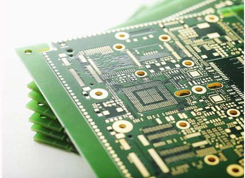
Solder mask: solder mask refers to the part of the board that needs to be painted with green oil; because it is a negative output, the actual effect of the part with solder mask is not painted with green oil, but tinned and silver-white!
Soldering layer: paste mask, which is used for machine patching, corresponds to the pads of all patch components, the size is the same as the toplayer/bottomlayer layer, and it is used to open the stencil to leak tin.
Key points: Both layers are used for soldering, which does not mean one is soldered and the other is green oil; then whether there is a layer refers to the green oil layer, as long as there is this layer on a certain area, it means this Is the area insulated with green oil? For the time being, I haven't encountered such a layer! The PCB board we drew has a solder layer on the pads by default, so the pads on the PCB board are made of silver-white solder. It is not surprising that there is no green oil; but the PCB we drew The wiring part on the board only has the toplayer or bottomlayer layer, and there is no solder layer, but the wiring part on the finished PCB board is coated with a layer of green oil.
That can be understood like this:
1. The solder mask layer means to open a window on the whole piece of solder mask green oil, the purpose is to allow soldering!
2. By default, the area without solder mask must be painted with green oil!
3. The paste mask layer is used for patch packaging! SMT package uses: toplayer layer, topsolder layer, toppaste layer, and toplayer and toppaste are the same size, topsolder is a circle larger than them. DIP package only uses: topsolder and multilayer layer (after some decomposition, I found that the multilayer layer is actually the topsolder, bottomlayer, topsolder, bottomsolder layer overlap in size), and topsolder/bottomlayer is a circle larger than toplayer/bottomlayer.
Question: Is the phrase "the copper skin layer corresponding to the solder layer is tinned or gold-plated only if there is copper" is correct?
This sentence was said by a person working in a PCB factory. What he meant was: if you want to make the part painted on the solder layer to be tinned, then the corresponding solder layer must have copper skin (ie : The area corresponding to the solder layer must have part of the toplayer or bottomlayer layer)! Now: I have come to a conclusion: "The copper skin layer corresponding to the solder layer has copper to be tinned or gold plated" is correct! The solder layer represents the area that does not cover the green oil!