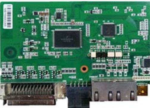
In the manufacture of electronic products, with the miniaturization and complexity of products, the assembly density of circuit boards is getting higher and higher, and the new generation of SMT assembly process that has been produced and widely used accordingly requires designers to Consider manufacturability. Once inadequate consideration in the design leads to poor manufacturability, it is necessary to modify the design, which will inevitably extend the introduction time and increase the introduction cost of the product, even if the PCB layout is slightly changed, the printed board and the SMT solder paste printing screen are re-made The cost of the board is as high as thousands or even tens of thousands of yuan, and the analog circuit even needs to be re-debugged. The delay in the introduction time may cause the company to miss good opportunities in the market and be strategically at a very disadvantageous position. However, if the product is reluctantly produced without modification, it will inevitably cause manufacturing defects in the product, or cause the manufacturing cost to soar, and the price paid will be even greater. Therefore, when an enterprise designs a new product, the sooner it considers the manufacturability of the design, the better it is for the effective introduction of new products.
2. What to consider when designing PCB

The manufacturability of PCB design is divided into two categories, one refers to the processing technology of producing printed circuit boards; the other refers to the assembly technology of circuit and structural components and printed circuit boards. Regarding the processing technology of the production of printed circuit boards, ordinary PCB manufacturers, due to their manufacturing capabilities, will provide designers with relevant requirements in great detail, which is relatively good in practice. According to the author’s understanding The second category that has not received enough attention in practice is the manufacturability design for electronic assembly. The focus of this article is also to describe the manufacturability issues that designers must consider at the stage of PCB design.
Manufacturability design for electronic assembly requires PCB designers to consider the following in the early stages of PCB design:
2.1 Appropriate selection of assembly methods and component layout
The choice of assembly method and component layout is a very important aspect of PCB manufacturability, which has a great impact on assembly efficiency, cost, and product quality. In fact, the author has come into contact with quite a few PCBs and considers some very basic principles. There are also shortcomings.
(1) Choose a suitable assembly method
Generally, according to the different assembly density of PCB, the recommended assembly methods are as follows:
What manufacturability issues should be considered in PCB design
As a circuit design engineer, you should have a correct understanding of the PCB assembly process flow you are designing, so that you can avoid making some principled mistakes. When choosing an assembly method, in addition to considering the assembly density of the PCB and the difficulty of wiring, it must also be based on the typical process flow of this assembly method and the level of the company's own process equipment. If the company does not have a better wave soldering process, then choosing the fifth assembly method in the above table may bring yourself a lot of trouble. Another point worth noting is that if you plan to implement a wave soldering process on the soldering surface, you should avoid arranging a few SMDs on the soldering surface to make the process complicated.
(2) Component layout
The layout of the components on the PCB has a very important impact on production efficiency and cost, and is an important indicator to measure the installability of the PCB design. Generally speaking, the components are arranged as evenly, regularly and neatly as possible, and arranged in the same direction and polarity distribution. The regular arrangement is convenient for inspection, is helpful to increase the patch/plug-in speed, and the uniform distribution is beneficial to the optimization of heat dissipation and welding process. On the other hand, in order to simplify the process, PCB designers must always know that on any side of the PCB, only a group soldering process of reflow soldering and wave soldering can be used. This is especially noteworthy when the assembly density is high and the PCB soldering surface must be distributed with more SMD components. The designer should consider which group soldering process to use for the mounted components on the soldering surface. The most preferred is to use the wave soldering process after the patch is cured, which can simultaneously solder the pins of the perforated device on the component surface; but the wave There are relatively strict constraints on soldering SMD components, and only chip resistors with sizes of 0603 and above, SOT, SOIC (pin spacing ≥ 1mm and height less than 2.0mm) can be soldered. For components distributed on the soldering surface, the pin direction should be perpendicular to the PCB transmission direction during wave soldering to ensure that the solder ends or leads on both sides of the component are dip-soldered at the same time. The arrangement order and spacing between adjacent components should also meet Wave soldering is required to avoid "shading effect". When wave soldering SOIC and other multi-pin components are used, tin-stealing pads should be set at the last two solder feet (1 on each side) in the tin flow direction to prevent continuous soldering.