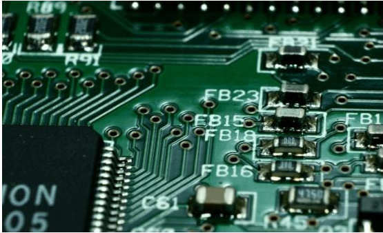
The concept of solder mask
The solder mask is the soldermask, which refers to the part of the PCB printed circuit board to be painted with green oil. In fact, this solder mask uses a negative output, so after the shape of the solder mask is mapped to the board, the solder mask is not painted with green oil, but the copper skin is exposed.
Process requirements for solder mask
The role of the solder mask in controlling solder defects during the reflow soldering process is important, and the PCB designer should minimize the spacing or air gaps around the pad features.
Although many process engineers would rather separate all pad features on the board with a solder mask, the pin spacing and pad size of fine-pitch components will require special considerations. Although solder mask openings or windows that are not partitioned on the four sides of the qfp may be acceptable, it may be more difficult to control the solder bridges between the component pins. For the solder mask of bga, many companies provide a solder mask that does not touch the pads, but covers any features between the pads to prevent solder bridges. Most surface mount PCBs are covered with a solder mask, but if the thickness of the solder mask is greater than 0.04mm ("), it may affect the application of solder paste. Surface mount PCBs, especially those using fine-pitch components, Both require a low-profile photosensitive solder mask.
Process production of solder mask

Solder mask materials must be used through liquid wet process or dry film lamination. Dry film solder mask materials are supplied in a thickness of 0.07-0.1mm (0.03-0.04"), which can be suitable for some surface mount products, but this material is not recommended for close-pitch applications. Few companies provide thin enough to meet Standard fine-pitch dry film, but there are several companies that can provide liquid photosensitive solder mask materials. Generally, the solder mask opening should be 0.15mm (0.006") larger than the pad. This allows a 0.07mm (0.003") gap on all sides of the pad. Low-profile liquid photosensitive solder masks are economical and are usually specified for surface mount applications, providing precise feature sizes and gaps.
Understanding of PCB solder mask window opening
The solder mask opening refers to the size of the part where the copper is exposed at the location that needs to be soldered, that is, the size of the part that is not covered with ink, and the cover line refers to the size and how much of the circuit part covered by the solder mask. If the distance of the cover line is too small, the line will be exposed during the production process.
Reasons for opening windows of PCB solder mask
1. Aperture opening: because many customers do not need ink to plug the hole, if the window is not opened, the ink will enter the hole. (This is for small holes) If the large hole is filled with ink, the customer cannot press the key. In addition, if it is a gold plate, the window must also be opened
2. PAD (that is copper) window opening: customers need welding, surface treatment (gold/tin spray, etc.).