1. PCB surface treatment: anti-oxidation, tin spray, lead-free tin spray, immersion gold, immersion tin, immersion silver, hard gold plating, full board gold plating, gold finger, nickel palladium gold OSP: lower cost, solderability Good, harsh storage conditions, short time, environmentally friendly technology, good welding, and smooth.
Tin spraying: The spray tin plate is generally a multi-layer (4-46 layer) high-precision PCB model. It has been used by many large domestic communication, computer, medical equipment, and aerospace companies and research units. ) Is the connecting part between the memory bar and the memory slot, all signals are transmitted through golden fingers.
Why "Paste Gold" on PCB Circuit Board
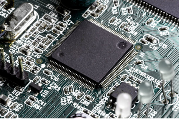
The gold finger is composed of many golden yellow conductive contacts. Because the surface is gold-plated and the conductive contacts are arranged like fingers, it is called "golden finger". The gold finger is actually coated with a layer of gold on the copper clad board through a special process, because gold has strong oxidation resistance and strong conductivity. However, due to the high price of gold, most of the memory is now replaced by tin plating. Since the 1990s, tin materials have been popularized. At present, the "golden fingers" of motherboards, memory and graphics cards are almost all used. Tin material, only part of the contact points of high-performance servers/workstations will continue to be gold-plated, which is naturally expensive.
2. Why use gold-plated plates
Why "Paste Gold" on PCB Circuit Board
As the integration level of IC becomes higher and higher, IC pins become more denser. The vertical spray tin process is difficult to flatten the thin pads, which brings difficulty to the placement of SMT; in addition, the shelf life of the spray tin plate is very short. The gold-plated board just solves these problems:
1. For the surface mount process, especially for 0603 and 0402 ultra-small surface mounts, because the flatness of the pad is directly related to the quality of the solder paste printing process, it has a decisive influence on the quality of the subsequent reflow soldering, so the whole board Gold plating is common in high-density and ultra-small surface mount processes.
2. In the trial production stage, due to factors such as component procurement, it is often not that the board is soldered immediately when it comes, but it is often used for several weeks or even months. The shelf life of the gold-plated board is better than that of lead. Tin alloy is many times longer, so everyone is happy to use it. Besides, the cost of gold-plated PCB in the sample stage is almost the same as that of lead-tin alloy board.
But as the wiring becomes denser, the line width and spacing have reached 3-4MIL.
Therefore, the problem of gold wire short circuit is brought about: As the frequency of the signal becomes higher and higher, the signal transmission in the multi-plated layer caused by the skin effect has more obvious influence on the signal quality.

The skin effect refers to: high frequency alternating current, the current will tend to concentrate on the surface of the wire to flow. According to calculations, the skin depth is related to frequency.
3. Why use Immersion Gold Board
Why "Paste Gold" on PCB Circuit Board
In order to solve the above problems of gold-plated boards, PCBs using gold-plated boards mainly have the following characteristics:
1. Because the crystal structure formed by immersion gold and gold plating is different, immersion gold will be golden yellower than gold plating, and customers will be more satisfied.
2. Because the crystal structure formed by immersion gold and gold plating is different, immersion gold is easier to weld than gold plating, and will not cause poor welding and cause customer complaints.
3. Because the immersion gold board only has nickel and gold on the pad, the signal transmission in the skin effect will not affect the signal on the copper layer.
4. Because immersion gold has a denser crystal structure than gold plating, it is not easy to produce oxidation.
5. Because the immersion gold board only has nickel and gold on the pads, it will not produce gold wires and cause slight shortness.
6. Because the immersion gold board only has nickel and gold on the pads, the solder mask on the circuit and the copper layer are more firmly bonded.
7. The project will not affect the distance when making compensation.
8. Because the crystal structure formed by immersion gold and gold plating is different, the stress of the immersion gold plate is easier to control, and for products with bonding, it is more conducive to bonding processing. At the same time, it is precisely because the immersion gold is softer than the gilding, so the immersion gold plate is not wear-resistant as the gold finger.
9. The flatness and stand-by life of the immersion gold board are as good as the gold-plated board.
4. Immersion gold board VS gold-plated board
In fact, the gold plating process is divided into two types: one is electroplating gold, the other is immersion gold.
For the gilding process, the effect of tinning is greatly reduced, and the tinning effect of immersion gold is better; unless the manufacturer requires binding, most manufacturers will now choose the immersion gold process! Generally, PCB surface treatments are as follows: gold plating (electroplating gold, immersion gold), silver plating, OSP, tin spraying (lead and lead-free), these types are mainly for FR-4 or CEM-3 For the board, the paper base material also has the surface treatment method of coating rosin; the poor tin application (poor tin eating) is considered if the production and material process reasons of the chip manufacturer such as solder paste are excluded.
Here is only for the PCB problem, there are the following reasons:
1. During PCB printing, whether there is an oil-permeable film surface on the PAN position, which can block the effect of tinning; this can be verified by a tin bleaching test.
2. Whether the lubrication position of the PAN position meets the design requirements, that is, whether the support function of the part can be guaranteed during the design of the pad.
3. Whether the pad is contaminated, this can be obtained by the ion contamination test; the above three points are basically the key aspects considered by PCB manufacturers.
Regarding the advantages and disadvantages of several methods of surface treatment, each has its own strengths and weaknesses!
In terms of gold plating, it can keep PCBs for a longer period of time, and is subject to small changes in the temperature and humidity of the outside environment (compared to other surface treatments), and generally can be stored for about one year; secondly, the surface treatment of tin spraying, OSP again, this A lot of attention should be paid to the storage time of the two surface treatments at ambient temperature and humidity.
Under normal circumstances, the surface treatment of immersion silver is a bit different, the price is also high, and the storage conditions are more demanding, so it needs to be packaged in sulfur-free paper! And the storage time is about three months! In terms of the effect of tinning, immersion gold, OSP, tin spraying, etc. are actually the same, and manufacturers mainly consider cost-effectiveness!