1. How to avoid crosstalk in PCB layout and design?
A changed signal (such as a step signal) propagates along the transmission line from A to B. A coupled signal will be generated on the transmission line CD. Once the changed signal ends, that is, when the signal returns to a stable DC level, the coupled signal will not exist, so crosstalk It only occurs in the process of signal transitions, and the faster the signal edge changes (conversion rate), the greater the crosstalk generated. The electromagnetic field coupled in the space can be extracted as a collection of countless coupling capacitors and coupling inductances. The crosstalk signal generated by the coupling capacitor can be divided into forward crosstalk and reverse crosstalk Sc on the victim network. These two signals have the same polarity; The crosstalk signal generated by the inductance is also divided into forward crosstalk and reverse crosstalk SL, and these two signals have opposite polarities. The forward crosstalk and reverse crosstalk generated by the coupled inductance and capacitance exist at the same time and are almost equal in size. In this way, the forward crosstalk signals on the victim network cancel each other due to the opposite polarity, and the reverse crosstalk polarity is the same, and the superposition is enhanced.
The modes of crosstalk analysis usually include default mode, three-state mode and worst-case mode analysis. The default mode is similar to the way we actually test the crosstalk, that is, the offending network driver is driven by a flip signal, and the victim network driver maintains the initial state (high level or low level), and then the crosstalk value is calculated. This method is more effective for crosstalk analysis of unidirectional signals. The tri-state mode means that the driver of the offending network is driven by a flip signal, and the tri-state terminal of the victim network is set to a high-impedance state to detect the size of the crosstalk. This method is more effective for two-way or complex topology networks. The worst-case analysis refers to keeping the driver of the victim network in the initial state, and the simulator calculates the sum of the crosstalk of all the default infringement networks to each victim network. This method generally only analyzes individual key networks, because there are too many combinations to be calculated and the simulation speed is relatively slow.

2. Is there any regulation on the copper area of the conduction band, that is, the ground plane of the microstrip line?
For microwave circuit design, the area of the ground plane has an impact on the parameters of the transmission line. The specific algorithm is more complicated (please refer to the relevant information of EESOFT by Angelen). In general PCB digital circuit transmission line simulation calculations, the ground plane area has no effect on the transmission line parameters, or ignores the impact.
3. In the EMC test, it was found that the harmonics of the clock signal exceeded the standard very seriously, but the decoupling capacitor was connected to the power supply pin. What aspects should be paid attention to in PCB design to suppress electromagnetic radiation?
The three elements of EMC are radiation source, transmission route and victim. The propagation path is divided into space radiation propagation and cable conduction. So to suppress harmonics, first look at the way it spreads. Power supply decoupling is to solve the propagation of conduction mode. In addition, necessary matching and shielding are also required.
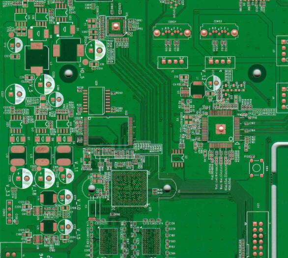
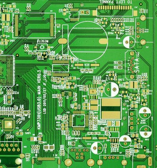
4. Among the products with 4-layer board design, why some are double-sided paving, and some are not?
There are several considerations for the role of paving: 1. Shielding; 2. Heat dissipation; 3. Reinforcement; 4. PCB processing requirements. So no matter how many layers of slabs are laid, we must first look at the main reasons. Here we mainly discuss high-speed issues, so we mainly talk about shielding. Surface paving is good for EMC, but copper paving should be as complete as possible to avoid islands. Generally, if there are many surface-layer device wiring, it is difficult to ensure the integrity of the copper foil, and it will also cause the problem of inter-segmentation of the inner layer signal. Therefore, it is recommended not to lay copper on the surface-layer devices or boards with many traces.