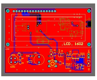
In PCB design and layout, assembly reliability, also known as process reliability, usually refers to the ability of PCBA not to be damaged by normal operations during assembly and soldering. If the design is improper, it is easy to damage or damage the soldered joints or components.
In PCB design and layout, assembly reliability, also known as process reliability, usually refers to the ability of PCBA not to be damaged by normal operations during assembly and soldering. If the design is improper, it is easy to damage or damage the soldered joints or components.
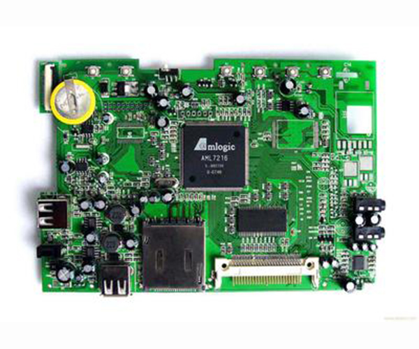
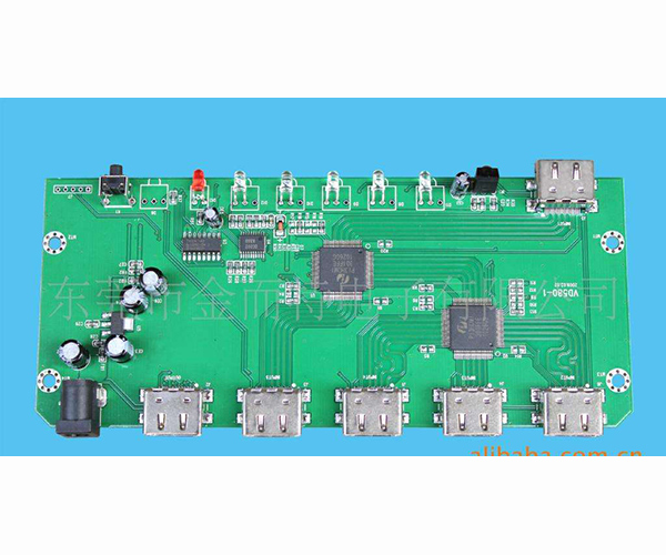
How to design PCBA assembly reliability
Stress-sensitive devices such as BGA, chip capacitors, and crystal oscillators are easily damaged by mechanical or thermal stress. In the PCB design and layout, the layout should be placed in a place where the PCB is not easily deformed, or reinforced design, or appropriate Measures to circumvent.
How to design PCBA assembly reliability

(1) In PCB design and layout, stress-sensitive components should be placed as far away as possible from places that are prone to bending during PCB assembly. In order to eliminate the bending deformation during the assembly of the daughter board, the connector that connects the daughter board with the mother board should be placed on the edge of the daughter board as much as possible, and the distance from the screws should not exceed 10mm.
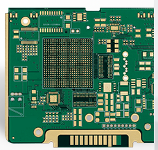
For another example, in order to avoid BGA solder joint stress cracking, it is necessary to avoid placing the BGA layout in a place that is prone to bending during PCB assembly. The poor design of BGA can easily cause its solder joints to crack when holding the board with one hand.
How to design PCBA assembly reliability
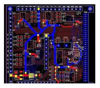
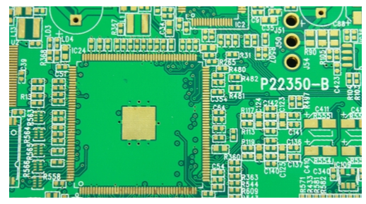
(2) Reinforce the four corners of the large-size BGA.
In PCB design and layout, when the PCB is bent, the solder joints at the four corners of the BGA receive the greatest force and are most likely to crack or break. Therefore, strengthening the four corners of the BGA is very effective in preventing the cracking of the corner solder joints. Special glue should be used for strengthening, or patch glue can be used for strengthening. This requires space for component layout, and the reinforcement requirements and methods should be indicated on the process documents.
How to design PCBA assembly reliability
In the PCB design and layout, the above two suggestions are mainly considered from the design aspect. On the other hand, the assembly process should be improved to reduce the generation of stress, such as avoiding the use of supporting tools for holding the board with one hand and mounting screws. Therefore, the design of assembly reliability should not be limited to the improvement of the layout of the components. The more important thing should be to reduce the stress of the assembly-adopt appropriate methods and tools, strengthen the training of personnel, and standardize the operation actions. Only in this way can the assembly stage be resolved. The problem of solder joint failure.