With the development of science and technology and the improvement of living standards, PCB boards are mainly facilities for connecting electronic components and electrical energy, which effectively help improve the level of automation and production labor rate. So do you know what are the cleaning steps for PCB boards? What are the maintenance methods? Let's take a look at it with the editor. The following is an introduction about "PCB cleaning process and maintenance measures".
Steps to clean up the residues after soldering on the PCB board wire module
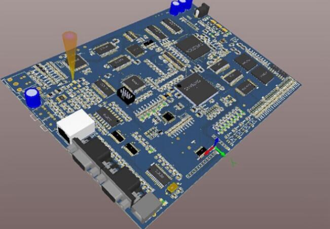
After the wireless data transmission module PCB board is soldered to the antenna SMA head, there will be some flux, rosin and other substances on the surface. At this time, you can use board washing water (commonly known as circuit board cleaner) to clean the wireless module after cleaning. To be clean, the cleaning steps are as follows:

1. Prepare special cotton swabs, washing water, rubber gloves, and masks. Because washing water is a chemical substance that is easy to evaporate, inhalation is irritating to the respiratory tract and lungs; in addition, washing water is corrosive to the skin, so Put on a mask, silicone gloves and other protective measures before cleaning.
2. Squeeze the special cotton swab into the mouth of the bottle containing the plate washer water. The bottle mouth will have the plate washer water squeezed out. Note: an appropriate amount is fine.
3. Take up the cotton swab and gently wipe the place where there is rosin residue near the welding SMA head. If it is not wiped clean, repeat the above procedure until it is wiped clean.
4. Put the clean wireless module into the designated box.
If there is dust and debris on the shielding cover of the wireless module, you can fold the special paper towel into about 3 layers, and use the folded paper towel to squeeze the mouth of the small bottle containing the plate washer water to squeeze out an appropriate amount of plate washer water. Wipe the top of the shielding cover from left to right at a time. If it is not clean, you can wipe it again.
Introduction to the maintenance and composition of the PCB board
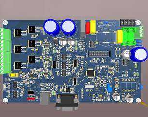
After the PCB is etched and cleaned, the surface must be coated and protected to improve the reliability of the solder joints. Coating the solder mask in the non-soldering area can prevent the solder from overflowing and cause bridging, and can play a role of moisture-proof after soldering. Coating on the surface of the pad to prevent oxidation of the pad.
(1) Solder mask. There are two types of solder mask graphic structures, one is the pad defined by the solder mask (SMD), and the other is the PCB pad defined by the non-solder mask (NSMD). Usually the solder mask of the NSMD pad is in computer CAD It is automatically formed in the design, and it covers graphics other than the pads. The margin of the solder mask from the soldering area is 0.1~0.25mm, and the part between the QFP soldering areas should be covered as much as possible.
The solder mask should be coated on a clean and dry bare copper board, otherwise there will be defects such as bubbles, wrinkles, and cracks in the solder mask during the soldering process. The SMD pad design can be appropriately enlarged, and the enlarged part can be used to increase the area covered by the solder mask, which is usually used in lead-free processes.
(2) Pad coating layer. In order to protect the pad and make it have good solderability and a longer validity period (6 months), it is necessary to add a coating on the surface of the pad. The pad coating layer usually adopts the following processes.
The above introductions about "Cleaning Steps of Residues after Soldering the Wireless Module PCB Board" and "Introduction to the Maintenance and Composition of the PCB Board", I hope to help you understand the "PCB cleaning process and maintenance measures".