Take the characteristic impedance of the transmission line on the PCB as an example: usually if the characteristic impedance is consistent everywhere on the same PCB interconnection line, such a transmission line on the PCB becomes high-quality.
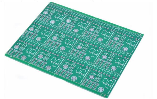
What kind of circuit board is called a controlled impedance circuit board?
A controlled impedance circuit board means that the characteristic impedance of all transmission lines on the PCB meets a unified target specification. It usually means that the characteristic impedance of all transmission lines is between 25Ω and 70Ω.
What is the main reason for the high impedance of the PCB circuit board? Or the quality of the PCB circuit board itself cannot be seen as a problem, but the problem (including impedance) increases with time, or what is the main reason for the unstable performance?
Please see the following professional academic analysis: Impedance-actually refers to the parameters of resistance and reactance, because the PCB circuit (bottom of the board) should consider plugging and installing electronic components, and considering the conductivity and signal transmission performance after plugging, it must be The lower the impedance, the better, and the resistivity should be lower than 1*10 per square centimeter to the minus 6th power.

On the other hand, during the production process, PCB circuit boards have to go through copper sinking, electrolytic tin plating (or chemical plating, or thermal spray tin), connector soldering and other links, and the materials used in this link must ensure the resistivity of the bottom, in order to ensure The overall impedance of the circuit board is so low that it meets the product quality requirements, otherwise the circuit board will not operate normally.
In addition, from the perspective of the electronics industry as a whole, PCB circuit boards are most prone to problems in the tinning process, and are the key link that affects impedance. Because the circuit board tinning process, chemical tinning technology is now popular to achieve tinning purposes., But as an employer in the electronics industry, we have been in contact with and observed in the electronics or electronics processing industry for more than 10 years. Looking at the domestic companies that can do chemical tinning (for PCB or electronic tinning), there are not many, because The electroless tinning process is a rising star in the country, and the technical level of the companies is uneven... For the electronics industry, according to industry surveys, the most fatal weakness of the electroless tin coating is its easy discoloration (easy to be oxidized or deliquescent), poor brazing properties leading to difficult soldering, and high impedance leading to poor electrical conductivity or instability in overall board performance., Easy long tin whiskers cause short circuit of PCB circuit and even burn out or catch fire.
It is reported that the first domestic research on chemical tin plating was Kunming University of Science and Technology in the early 1990s, followed by Guangzhou Tongqian Chemical (enterprise) in the late 1990s. Up to now, the industry has recognized that these two institutions are The best. Among them, according to our contact screening surveys, experimental observations and long-term endurance tests of many companies, it is confirmed that the tin-plated layer of Tongqian Chemical is a pure tin layer with low resistivity, and the quality of conductivity and brazing can be guaranteed to a high level. No wonder they dare to guarantee to the outside that the coating can keep its color for one year, no blistering, no peeling, and permanent tin whisker without any sealing and anti-tarnish protection.
Later, when the entire social production industry developed to a certain extent, many subsequent participants often copied each other. In fact, a considerable number of companies themselves did not have the R&D or initiative capabilities themselves. Therefore, many products and their users’ electronic products (circuit boards) The bottom of the board or the overall electronic product) performance is poor, and the main reason for the poor performance is the impedance problem, because when the unqualified electroless tin technology is in use, it is actually the tin plated on the PCB circuit board It is not really pure tin (or pure metal element), but tin compound (that is, it is not a metal element at all, but a metal compound, oxide or halide, or more directly a non-metal substance) or tin A mixture of compound and tin metal element, but it is difficult to find with the naked eye...
And because the main circuit of the PCB circuit board is copper foil, the solder joint of the copper foil is the tin-plated layer, and the electronic components are soldered on the tin-plated layer by solder paste (or solder wire). In fact, the solder paste is The molten state soldered between the electronic component and the tin plating layer is metal tin (ie, a metal element with good conductivity), so it can be simply pointed out that the electronic component is connected to the copper foil at the bottom of the PCB through the tin plating layer, so The purity of the tin plating and its impedance are the key; but before the electronic components are plugged in, when we directly use the instrument to detect the impedance, in fact, the two ends of the instrument probe (or called the test lead) first touch the bottom of the PCB board. The tin-plated layer on the surface of the copper foil is then connected to the copper foil at the bottom of the PCB board to communicate the current. Therefore, tin plating is the key, the key that affects the impedance and the key that affects the performance of the entire PCB, and it is also the key that is easy to be ignored. In addition, it is well known that, except for the simple substance of metal, its compounds are poor electrical conductors or even non-conductive (in addition, this is also the key to the existence of distributed capacity or spreading capacity in the circuit), so there is this kind of similar conductive but in the tin plating layer. In the case of non-conductive tin compounds or mixtures, the existing resistivity or the resistivity after the electrolysis reaction due to future oxidation or moisture and the corresponding impedance are quite high (enough to affect the level or signal transmission in the digital circuit, ) And its characteristic impedance is not consistent. So it will affect the performance of the circuit board and the whole machine.
Therefore, as far as the current social production phenomenon is concerned, the coating material and performance on the bottom of the PCB board are the most important and most direct reasons affecting the characteristic impedance of the entire PCB. Variability, so the worrying impact of its impedance has become more invisible and variable. The main reasons for its concealment are: firstly, it cannot be seen by the naked eye (including its changes), and secondly, it cannot be measured constantly, because it has The variability changes with time and environmental humidity, so it is always easy to be ignored. Or pass the reason wrong. Therefore, after knowing the cause of the high impedance, solving the plating problem is the key to the impedance problem.