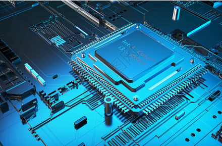
For designers who are beginners to circuit boards, only after fully understanding the production process of circuit boards can they design circuit boards better. Therefore, it is necessary to have a certain understanding of circuit board production.
The simple production process of the circuit board is as follows:
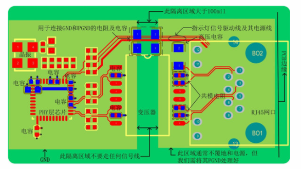
The first step: Design a circuit board schematic diagram that meets the requirements according to the needs of the circuit and the required functions. The main basis of the circuit board schematic design is that the performance and functions of various components need to be reasonably matched. The function of the circuit board can be clearly and accurately reflected through the drawing of the circuit board. The design of the circuit board schematic diagram is the first and most important step in the production of the circuit board, and we should pay full attention to it.
Step 2: After the PCB schematic design is completed, the next thing to do is to effectively package the components through the PROTEL software. So that we can better realize the grid of circuit board components with the same appearance and size.

Step 3: Generate the drawing of the circuit board. After it is generated on the computer, we need to place the position of each component according to the size of the specific PCB panel to ensure that the leads of the components distributed on the circuit board are not The phenomenon of crossing occurs. Finally, we need to perform DRC inspection on the circuit board. The purpose of this operation is to avoid crossover errors in the pins or leads during wiring.
Step 4: Use special carbon paper to print out the designed PCB diagram through an inkjet printer, and then press the side with the printed circuit diagram against the copper plate, and finally put it on the heat exchanger for hot printing. Glue the circuit diagram ink on the carbon paper to the copper plate.
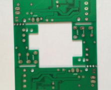
The fifth step: circuit board manufacturing. Prepare the solution, mix sulfuric acid and hydrogen peroxide in a ratio of 3:1, then put the copper plate containing ink stains into it, wait for about three to four minutes, wait until all the copper plate except the ink stains are corroded, then remove the copper plate, And then rinse off the solution with clean water.
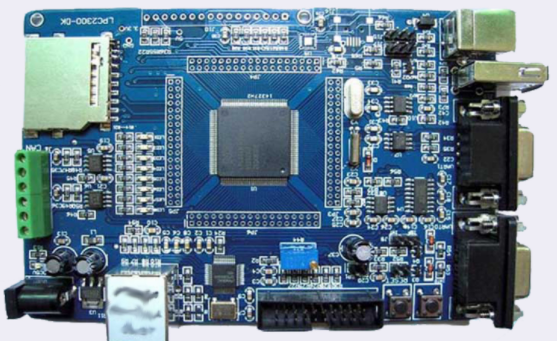
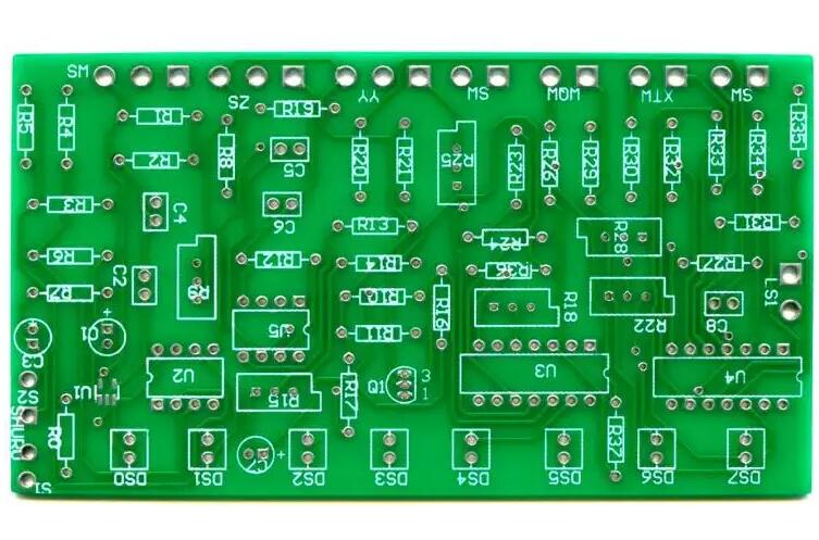
Step 6: Punching the circuit board. First, we need to use a hole drilling machine to drill the holes left on the copper clad board one by one. After the operation is completed, we need to place each component from the back of the copper clad board. Two or more pins are introduced, and then welding tools are needed to solder the components to the copper clad board.
The seventh step: After the welding work is completed, the next operation we need is to conduct a comprehensive test operation on the circuit board, if some conditions are found on the circuit board during the test process. At this time, it is necessary to analyze the PCB schematic diagram to determine the location of the problem. After finding the problem, you can re-weld and replace the components. After the test has no problems, the production of the circuit board is ok!