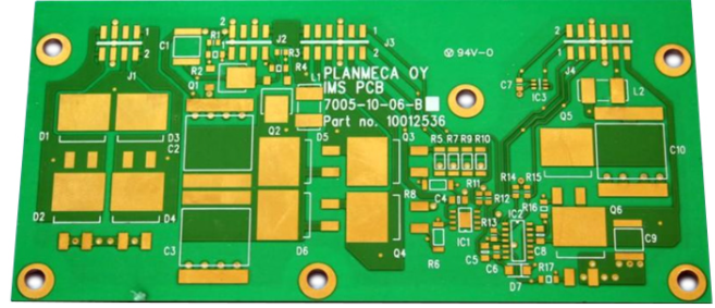
The layout of components must not only meet the requirements of the electrical performance and mechanical structure of the whole machine, but also meet the requirements of the SMT production process. As product quality problems caused by design are difficult to overcome in production, PCB design engineers are required to have a basic understanding of the process characteristics of SMT, and design the layout of components according to different processes. The correct design can minimize welding defects.
1. Circuit design requirements for component layout
The component layout has a great influence on the performance of the PCB. When designing the circuit, the large circuit is generally divided into unit circuits, and the position of each unit circuit is arranged according to the flow direction of the circuit signal, avoiding the intersection of input/output and high and low levels; the flow direction must be regular, and the direction should be kept as consistent as possible. Make it easy to find faults.

2. SMT process requirements for component layout design
The layout of components should be designed according to SMT production equipment and process characteristics. Regardless of the process, such as reflow soldering and wave soldering, the layout of the components is different; when double-sided reflow soldering, there are also different requirements for the layout of the main surface and the auxiliary surface, and so on.
How to make a reasonable layout of PCB design and what are the requirements
(1) The distribution of PCB components should be as even as possible.
(2) Similar components should be arranged in the same direction as much as possible, and the characteristic directions should be consistent to facilitate mounting, welding and testing.
(3) A certain maintenance gap should be left around the large components, and the size of the heater head of the SMD rework equipment can be operated.
(4) The heating element should be as far away as possible from other components, generally placed in the corners and in a ventilated position in the chassis.
(5) Keep temperature-sensitive components away from heating components.
(6) The layout of components and parts that need to be adjusted or frequently replaced, such as potentiometers, adjustable inductance coils, variable capacitors, micro switches, fuses, buttons, plugs, etc., should be considered for the overall structure requirements, Placed in a position that is easy to adjust and replace.
(7) Fixing holes should be provided near the terminals, plug-in parts, the center of the long series of terminals and the parts that are often subjected to force. There should be corresponding space around the fixing holes to prevent deformation due to thermal expansion and warping during wave soldering. From the phenomenon.
(8) For some parts (such as transformers, electrolytic capacitors, varistors, bridge stacks, radiators, etc.) that require secondary processing due to large volume (area) tolerances and low precision, the distance between them and other components Add a certain amount of surplus on the basis of the original setting.
(9) Do not place valuable components on the corners, edges of the PCB or close to the connectors, mounting holes, slots, cutting, gaps and corners of the jigsaw board. These locations are high stress areas of the printed board, which are easy to cause Cracks or cracks in solder joints and components.
Whether the bureau is reasonable or not will directly affect the wiring effect, so a reasonable PCB layout is the first step to a successful PCB design.