Vector imaging technology is a graphic location search technology, which can improve the accuracy, speed and reliability of component recognition and positioning during the PCB board assembly process. Vector imaging technology can be easily used in a dedicated production environment. For PCBA OEMmanufacturers and electronic manufacturing service (EMS) suppliers, the key is to improve component inspection capabilities and reduce overall manufacturing costs.
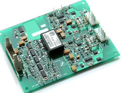
In the hardware maintenance of various electronic equipment circuit boards and other hardware, the detection of various common components on the board is a compulsory course for learners of electronic maintenance. As the density of current circuit boards continues to increase and packaging continues to shrink, the past inspection methods can no longer meet the requirements of high-speed production, and a new vector inspection method has emerged. In the PCB assembly process, vector imaging technology is used to identify and place components, which can improve the accuracy, speed and reliability of detection.
The performance of each equipment on the PCB assembly production line varies according to demand. The production requirements of the manufacturer plus the higher density of the circuit board, more complex layout technology and smaller components, etc., all give solder paste Coating, component placement, reflow soldering, and inspection of these processes have brought great difficulties.

The increase in output and the decrease in packaging have increased the difficulty of detection, making the current detection and analysis methods unable to keep up with the needs of the development of the industry. In the past few years, people have developed many different types of methods to inspect printed circuit board assembly, such as X-ray inspection, laser scanning, automatic optical inspection (AOI), and X-ray/AOI hybrid inspection. Among these methods, only AOI has On-line inspection capabilities, while other methods can only be used in a small range, such as laser scanning for solder paste inspection, and two-dimensional or three-dimensional X-rays for detecting the interconnection of solder balls in area array devices.
The basic principle of automatic optical inspection is to use software tools to enable the operator to find and determine the location of the components, which can detect leaded devices, chip scale package (CSP) and ball grid array (BGA) packaged devices, etc. Traditional AOI relies on the analysis of the pixel grid value to confirm the position of the components on the circuit board. This method is also called gray-scale correlation method. It compares the gray-scale model or reference image of the component with the actual components on the board. For the model to be searched, the image processing system searches for an exact matching component by counting the number of pixels. If it is found, the position of the component is also known. Since the system will constantly detect some new components, the reference graphics may often change in order to adapt to these new component shapes.
When the PCB component is rotated by an angle relative to the reference model or the size is not consistent, the pixel grid analysis method will be problematic. Similarly, the color, lighting, and background of the product are also important. If it changes greatly, it may be difficult or impossible to find a matching model.
Vector imaging technology
Vector imaging technology uses composite images as a teaching reference model to ensure that no errors occur. Vector imaging does not require pixel analysis. It relies on the intersection vector that defines the shape of the component. The vector is determined by the direction and inclination. In vector imaging technology, a square is equivalent to four line segments, and a football is equivalent to two arcs.
The vector imaging technology uses a Windows operating system and a high-resolution digital camera. The system uses statistical process control (SPC) software and a comprehensive component graphic library based on the components assembled on the circuit board and needs to be inspected, measured and analyzed. It can Convert Gerber, CAD or ASCII/Centrid data into machine code.
In order to obtain the best contrast and imaging clarity, several light sources are needed. The light source, color combination and light intensity are selected by the program during inspection to achieve the best visual effect. In order to ensure the correctness of recognition, the height of the component must be less than 8mm (from the surface of the PCB board to the top of the component).
Because vector imaging technology uses geometric information, it has no effect on whether the component rotates, and the size of the obtained figure is consistent with the reference model, and it has nothing to do with changes in product color, lighting, and background. The vector imaging inspection is carried out in three parts:
The vector imaging system finds the main features on the component image map and separates them, and then measures these salient features, including shape, size, angle, radian and brightness, etc.;
Check the spatial relationship between the composite image and the main features of the component under test;
Finally, regardless of the component's rotation angle, size or overall appearance relative to its background, its x, y and θ values on the circuit board can be determined by calculation.
Different from other inspection methods, vector imaging technology can adapt to every component on the circuit board as long as a reference model is created, regardless of its shape, size and orientation. When the component model is transferred from one visual inspection device to another device with a different optical system, the size of the image obtained will change, but the system can automatically handle the change at this time.
In addition, vector imaging technology can also adapt to changes in the appearance of PCB components, additional features on components, or part of a component that is hidden and obscured due to overlap. Traditional pixel grid systems generally cannot analyze the position of the obscured component.