In the design and manufacturing process of high-speed PCB circuit boards, engineers need to start with wiring and component settings to ensure that this PCB board has good signal transmission integrity. In today's article, we will introduce some wiring techniques that are often used in PCB signal integrity design for newcomers engineers, hoping to bring some help to newcomers' daily study and work.
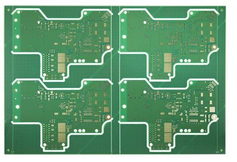
In the design process of high-speed PCB circuit boards, the cost of the printed circuit of the substrate is proportional to the number of layers and the surface area of the substrate. Therefore, under the premise of not affecting the system function and stability, engineers should use the least number of layers to meet the actual design needs, which will inevitably increase the wiring density. In the PCB wiring design, the greater the wiring width Fine, the smaller the interval, the greater the crosstalk between signals, and the smaller the transmission power. Therefore, the selection of trace size must consider various factors.
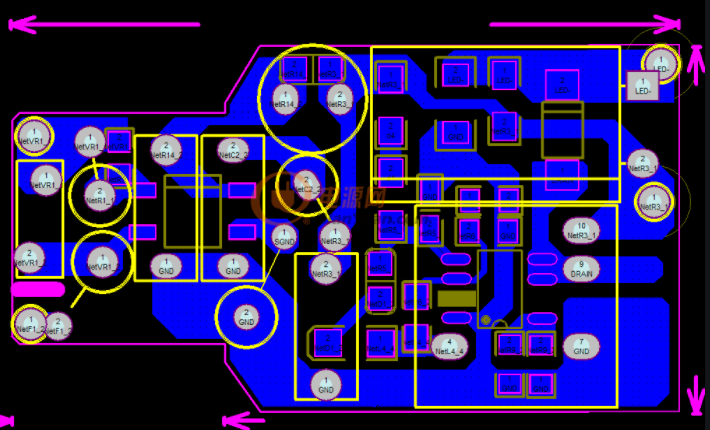
In the PCB layout design process, the principles that engineers need to follow are mainly as follows:

First of all, designers should minimize the bending of the leads between the pins of the high-speed circuit devices during the wiring process, and use 45? fold lines to reduce the external reflection and mutual coupling of high-frequency signals.
Secondly, when performing the wiring operation of the PCB board, the designer should shorten the lead between the pins of the high-frequency circuit device as much as possible and the inter-layer alternation of the lead between the pins. High-frequency digital signal traces should be as far away as possible from analog circuits and control circuits.
In addition to the precautions for PCB wiring mentioned above, engineers also need to be cautious when dealing with differential signals. Because the differential signal has the same amplitude and the same direction, the magnetic fields generated by the two signal lines cancel each other out, which can effectively reduce EMI. The spacing of the differential lines often leads to changes in the differential impedance, and the inconsistency of the differential impedance will seriously affect the signal integrity. Therefore, in actual differential wiring, the difference in length between the two signal lines of the differential signal must be controlled at the time of the rising edge of the signal. Within 20% of the electrical length. If conditions permit, the differential wiring must meet the back-to-back principle and be in the same wiring layer. In the setting of the line spacing of differential wiring, engineers need to ensure that it is at least equal to or greater than 1 times the line width. The distance between differential traces and other signal lines should be greater than three times the line width.
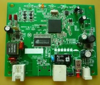
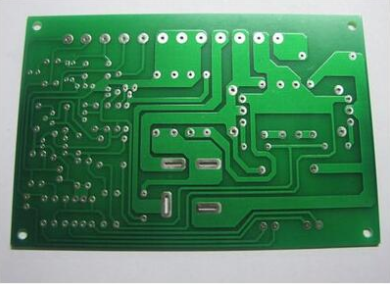
After PCBA board components are soldered (including reflow soldering and wave soldering), small light green bubbles will appear around individual solder joints. In severe cases, there will be fingernail-sized bubbles, which not only affects the appearance quality, but also Will affect the performance, the above-mentioned defects are also one of the frequent problems in the welding industry.
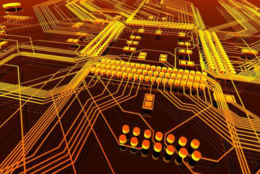
PCBA components after soldering
The fundamental reason for the blistering of the solder mask is the presence of gas and water vapor between the solder mask and the PCB substrate, where a trace amount of gas or water vapor will be entrained in it during different processes. When the soldering high temperature is encountered, the gas expands This leads to delamination between the solder mask and the PCB substrate. During soldering, the temperature of the pad is relatively high, so bubbles first appear around the pad. The following reasons will cause moisture to be entrained on the PCB:
1. In the process of electronic processing, PCB often needs to be cleaned and dried before doing the next process. If it is etched, it should be dried before applying solder mask. If the drying temperature is not enough at this time, water vapor will be entrained into the next process, and bubbles will appear when high temperature is encountered during welding.
2. The storage environment before PCB processing is not good, the humidity is too high, and whether it is dried in time during soldering.
3. In the wave soldering process, water-containing flux is often used now. The water vapor in the flux will enter the inside of the PCB substrate along the hole wall of the through hole, and the water vapor first enters around the pad, and after the soldering high temperature is encountered Will produce bubbles.
Solution:
1. All links should be strictly controlled. The purchased PCB should be put into the warehouse after inspection. Usually, the PCB should not be blistered after 260 degree Celsius/10s.
2. PCB should be stored in a ventilated and dry environment, and the storage period should not exceed 6 months.
3. The PCB is pre-baked (120±5) degree Celsius/4h in the oven before soldering.
4. The preheating temperature in wave soldering should be strictly controlled. Before entering wave soldering, it should reach 100 degree Celsius~150 degree Celsius. When using water-containing flux, the preheating temperature should reach 110 degree Celsius~155 degree Celsius to ensure that the water vapor can be completely volatilized. .