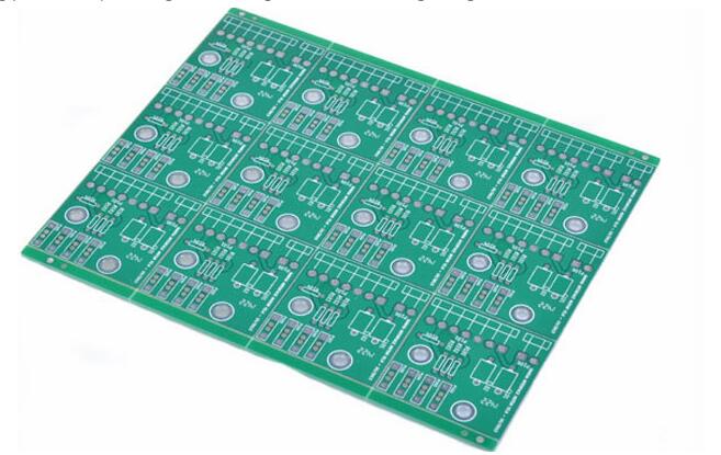
In the design of high-speed PCB analog signal chain, printed circuit boards, PCB layout and routing need to consider many options, some options are more important than others, and some options depend on the application. The final answer varies, but in all cases, design engineers should try to eliminate errors in best practices and not overly care about every detail of layout. This article recommended for you today will start with the exposed pad and describe in turn the four parts of decoupling and layer capacitance, layer coupling, and ground separation.
Exposed pad
The exposed pad (EPAD) is sometimes overlooked, but it is very important to give full play to the performance of the signal chain and to adequately dissipate heat from the device.
The exposed pad, which ADI calls pin 0, is the pad under most devices today. It is an important connection, and all internal grounding of the chip is connected to the center point under the device through it. I wonder if you noticed that many converters and amplifiers currently lack ground pins because of the exposed pad.
The key is to properly fix (ie solder) this pin to the PCB circuit board to achieve a reliable electrical and thermal connection. If this connection is not strong, confusion will occur, in other words, the design may be invalid.
achieve the best connection

There are three steps to achieve the best electrical and thermal connection with the exposed pad
First, where possible, the exposed pads should be replicated on each PCB layer. The purpose of this is to form a dense thermal connection with all grounding and grounding layers to quickly dissipate heat. This step is related to high-power devices and applications with high channel counts. Electrically, this will provide good equipotential bonding for all ground planes.
It is even possible to duplicate the exposed pad on the bottom layer, which can be used as a ground point for decoupling heat dissipation and a place to install a heat sink on the bottom side.
Second, divide the exposed pad into multiple identical parts, like a chessboard. Use a wire mesh cross grid on the open exposed pad, or use a solder mask. This step can ensure a stable connection between the device and the PCB circuit board. During the reflow assembly process, it is impossible to determine how the solder paste flows and ultimately connects the device to the PCB. Connections may exist, but they are not evenly distributed. You may only get one connection, and the connection is small, or worse, it is in the corner. Dividing the exposed pad into smaller parts can ensure that each area has a connection point to achieve a more reliable and evenly connected exposed pad.
Third, make sure that all parts have vias connected to the ground. Each area is usually large enough to place multiple vias. Before assembling, be sure to fill each via with solder paste or epoxy. This step is very important to ensure that the exposed pad solder paste will not reflow into these via holes and affect the correct connection.
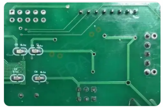
Decoupling and layer capacitance
Sometimes engineers will ignore the purpose of using decoupling, and just disperse many capacitors of different sizes on the circuit board, so that the lower impedance power supply is connected to the ground. But the question remains: how much capacitance is needed? Many related documents indicate that many capacitors of different sizes must be used to reduce the impedance of the power transmission system (PDS), but this is not entirely correct. On the contrary, it is only necessary to select the correct size and the correct type of capacitor to reduce the PDS impedance.
layer coupling
Some PCB layouts inevitably have overlapping circuit layers. In some cases, it may be a sensitive analog layer (such as power, ground, or signal), and the layer below is a high-noise digital layer.
This is often overlooked because the high-noise layer is on another layer-below the sensitive analog layer. However, a simple experiment can prove that this is not the case. Take a certain layer as an example, inject signals at any layer. Then connect another layer and cross-couple the adjacent layer to the spectrum analyzer.
separate ground
The most frequently asked question by analog signal chain designers is: Should the ground plane be divided into AGND and DGND ground planes when using an ADC? The short answer is: it depends. The detailed answer is: usually no separation. why not? Because in most cases, blindly separating the ground plane will only increase the inductance of the return path, and it does more harm than good.