Current electronic products are changing with each passing day, requiring high-density assembly of circuit boards. It is a historical necessity to replace through-hole insertion (THT) with surface mounting (SMT). Therefore, printed board technology is rapidly moving towards high-density and multilayering. develop. The reasonable design of printed boards is the key to SMT technology, as well as the guarantee of SMT process quality, and helps to improve production efficiency. This article describes some manufacturing process issues that need to be considered when designing surface mount PCBs, and provides a reference for PCB designers.
1 Introduction
In the manufacture of electronic products, with the miniaturization and complexity of products, the assembly density of circuit boards is getting higher and higher, and the new generation of SMT assembly process that has been produced and widely used accordingly requires designers to Consider manufacturability. Once inadequate consideration in the design leads to poor manufacturability, it is necessary to modify the design, which will inevitably extend the introduction time and increase the introduction cost of the product, even if the PCB layout is slightly changed, the printed board and the SMT solder paste printing screen are re-made The cost of the board is as high as thousands or even tens of thousands of yuan, and the analog circuit even needs to be re-debugged. The delay in the introduction time may cause the company to miss good opportunities in the market and be strategically at a very disadvantageous position.
2, the content considered in PCB design
The manufacturability of PCB design is divided into two categories, one refers to the processing technology of the production of printed circuit boards; the other refers to the assembly technology of the circuit and structural components and the printed circuit board.

Regarding the processing technology of the production of printed circuit boards, the general PCB manufacturer, due to its manufacturing capacity, will provide designers with relevant requirements in great detail, which is relatively good in practice. According to the author It is understood that the second category that has not received enough attention in practice is the manufacturability design for PCBA assembly. The focus of this article is also to describe the manufacturability issues that designers must consider at the stage of PCB design.
Manufacturability design for PCBA assembly requires PCB designers to consider the following at the early stage of PCB design:
2.1 Appropriate choice of assembly method and component layout
The choice of assembly method and component layout is a very important aspect of PCB manufacturability, which has a great impact on assembly efficiency, cost, and product quality. In fact, the author has come into contact with quite a few PCBs and considers some very basic principles. There are also shortcomings.
(1) Choose the right assembly method
Generally for the different assembly density of PCB, the recommended assembly methods are as follows:
As a circuit design engineer, you should have a correct understanding of the PCB assembly process flow, so that you can avoid making some principled mistakes. When choosing an assembly method, in addition to considering the assembly density of the PCB and the difficulty of wiring, it must also be based on the typical process flow of this assembly method, and consider the level of the company's own process equipment. If the company does not have a better wave soldering process, then choosing the fifth assembly method in the above table may bring yourself a lot of trouble. Another point worth noting is that if you plan to implement a wave soldering process on the soldering surface, you should avoid arranging a few SMDs on the soldering surface to make the process complicated.
(2) Component layout
The layout of the components on the PCB has a very important impact on production efficiency and cost, and is an important indicator to measure the installability of the PCB design. Generally speaking, the components are arranged as evenly, regularly and neatly as possible, and arranged in the same direction and polarity distribution. The regular arrangement is convenient for inspection, is helpful to increase the patch/plug-in speed, and the uniform distribution is beneficial to the optimization of heat dissipation and welding process. On the other hand, in order to simplify the process, PCB designers must always know that on any side of the PCB, only a group soldering process of reflow soldering and wave soldering can be used. This is especially worth noting when the assembly density is high and the soldering surface of the PCB must be distributed with more SMD components.
2.2 The necessary clamping edges, positioning marks, and process positioning holes for automated production must be arranged on the PCB.
At present, PCBA assembly is one of the industries with the highest degree of automation. The automation equipment used in production requires the automatic transmission of PCB. This requires that in the transmission direction of the PCB (usually the long-side direction), there should be no less than 3- The 5mm wide clamping edge facilitates automatic transmission and prevents components close to the edge of the board from being unable to be automatically assembled due to clamping.
The function of the positioning mark is that for the currently widely used optical positioning assembly equipment, the PCB is required to provide at least two to three positioning marks for the optical identification system to accurately position the PCB and correct the PCB processing errors. Among the commonly used positioning marks, two marks must be distributed on the diagonal of the PCB. The selection of positioning marks generally uses standard graphics such as solid round pads. For easy identification, there should be an open area without other circuit features or marks around the mark. The size should preferably not be less than the diameter of the mark. The mark should be 5mm away from the edge of the board. above.
In the manufacturing of the PCB itself, as well as in the semi-automatic plug-in and ICT testing processes in the assembly, it is necessary for the PCB to provide two to three positioning holes in the corners.
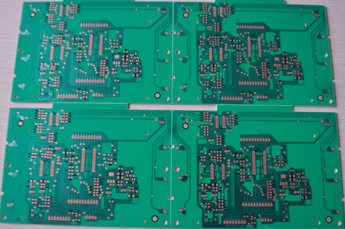
2.3 Reasonable use of puzzles to improve production efficiency and flexibility.
When assembling PCBs with small or irregular shapes, there are many restrictions. Therefore, the method of splicing several small PCBs into PCBs of suitable size is generally used for assembly, as shown in Figure 5. Generally, for PCBs with a single side size less than 150mm, you can consider using the boarding method. Through two, three, four, etc., the size of the large PCB can be assembled to the appropriate processing range, usually 150mm~250mm in width and 250mm~350mm in length. The PCB is a more suitable size in automated assembly.
The above are some of the main principles that should be considered when designing PCBs. In PCB manufacturability design for PCBA assembly, there are still quite a few detailed requirements.