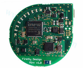
The following will introduce the purpose of nickel (Ni) plating on PCB boards:
"Nickel" is called [Nickel] in English, and the chemical element symbol is [Ni]. Because of its excellent physical, mechanical and chemical properties, "Nickel" has many applications in engineering and industry, such as anti-corrosion, Increase the application of hardness, abrasion resistance and magnetism. It is mainly used in alloy formulations, such as nickel steel, nickel chromium steel, nickel copper, etc. to increase its corrosion resistance and oxidation resistance. Because of its good oxidation resistance, it was often used to make money in the early days.
The so-called good anti-oxidation of nickel? Special note is needed here. In fact, the activity of "nickel" itself to "oxygen" is quite high, that is to say, "nickel" itself is also easy to oxidize, but because of the oxides (NiO, Ni(OH) 2) It has excellent fineness and can form a film to cover itself to isolate itself from continuing contact with the air, so it can resist oxidation, which means that nickel will oxidize itself to form a protective film before it can protect itself and the bottom metal from Yu continued to oxidize.
Therefore, "nickel" is often used for electroplating on other metal surfaces to protect the underlying metal from contact with air and cause oxidation. However, the plating layer must be "defect-free". To a certain degree of protection, in the early nickel plating process, because the process is not very mature, small holes often occur, so that the underlying metal material under the plating layer cannot be completely sealed, resulting in the oxidation of the underlying metal after nickel plating. The problem, and the current PCB nickel plating process has become mature day by day, usually a hole sealing agent is added to the plating bath to solve the problem of porosity.

In addition to the effect of preventing oxidation on the metal surface, nickel plating can also enhance the following mechanical properties:
1. Tensile strength
2. Elongation
3. Hardness
4. Internal stress (internal)
5. Fatigue life
6. Hydrogen embrittlement
In addition, nickel plating also has good resistance to chemical corrosion, and is often used in the chemical, petroleum, food and beverage industries to prevent corrosion, prevent product contamination, and maintain product purity. However, it should be noted that when the nickel oxide protective film is invaded by the chloride solution, it will form pinhole corrosion. Generally, the nickel plating layer will not be too problematic in neutral or alkaline solutions, but most of the problems are encountered. Minerals will be corroded.
The main purpose of plating "nickel" on the ENIG (nickel immersion gold) PCB circuit board is to prevent the migration and diffusion between copper and gold, as a barrier layer and corrosion resistance The protective layer protects the copper layer from oxidation, and can also prevent the conductivity and solderability from cracking. According to the recommendations of IPC-4552 on ENIG’s nickel plating, its thickness must be at least 3µm (micrometer)/118µ" to achieve Protective effect. In the process of soldering or SMT reflow, the nickel layer will combine with the tin in the solder paste to form Ni3Sn4 intermetallic compound (IMC, InterMetallic Compound). Although the strength of this IMC is not as strong as that of OSP surface treatment The generated Cu6Sn5 is already sufficient to meet the needs of most current products.
In addition, in order to achieve a certain mechanical strength for the pins of electronic parts, "brass" is often used instead of "pure copper" as the substrate. However, because brass contains a large amount of "zinc", it will greatly hinder the solderability, so it is not possible to plate tin directly on the brass, and a layer of "nickel" must be plated as a barrier layer. In order to successfully complete the task of welding.
Please note: Do not plate tin directly on the brass surface, because the brass is a copper-zinc alloy, otherwise the copper will peel off directly after remelting, and there will be false welding.
Is it possible to use nickel plating directly for soldering? The answer is basically no, because "nickel" is also very easy to passivation (Passivation) in the atmospheric environment, and it will also have an extremely adverse effect on the solderability, so generally a layer of pure tin is plated on the outside of the nickel layer. Improve the solderability of the part feet. Unless the packaging of the finished parts can ensure that the air is isolated, and the user can ensure that the nickel layer is not oxidized before welding, once the nickel layer is oxidized, even if it is welded, its welding strength will continue to deteriorate and eventually break.
In order to prevent the migration and diffusion of zinc and tin in brass, in addition to pre-plating a layer of nickel, some people also choose to pre-plating pure copper as a barrier layer and a protective layer against corrosion., And then tinned to strengthen the soldering ability.
It is common for some tin-plated parts to oxidize after being placed for a period of time. Most of them are caused by no pre-plated copper or pre-nickel, or the thickness of the pre-plated layer is not enough to prevent the above problems.
If the purpose of tinning is to strengthen the solder, matte tin plating is generally recommended instead of bright tin plating.
According to the requirements of IPC4552, the thickness of the gold layer of ENIGPCB circuit board is recommended to fall between 2µ"~5µ" (0.05µm~0.125µm), and the thickness of the chemical nickel layer should fall between 3µm(118µ")~6µm(236µ") .