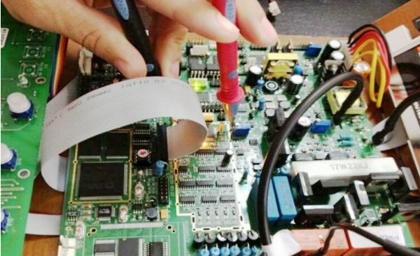
The high-frequency board wiring rules of the PCB factory include the component arrangement rules, the layout principle according to the signal direction, the prevention of electromagnetic interference, the suppression of thermal interference, and the layout of adjustable components.
1. Component arrangement rules
High-frequency PCB board wiring rules 1. Under normal conditions, all components should be arranged on the same surface of the printed circuit. Only when the top components are too dense, can some devices with limited height and low heat generation, such as stickers Chip resistors, chip capacitors, and ICs are placed on the bottom layer.
2. Under the premise of ensuring electrical performance, the components should be placed on the grid and arranged in parallel or perpendicular to each other to be neat and beautiful. In general, they are not allowed to overlap; the arrangement of components should be compact, and the input and output components should be as far away as possible.
3. There may be a relatively high potential difference between certain components or wires, and their distance should be increased to avoid accidental short circuits due to discharge and breakdown.
4. The components with high voltage should be placed as far as possible in a place that is not easy to reach during debugging.
5. Components located at the edge of the board, at least 2 board thickness distance from the edge of the board
6. The components should be evenly distributed and densely distributed on the entire board surface.
2. According to the principle of signal layout
1. The positions of each functional circuit unit are usually arranged one by one according to the signal flow, and the core components of each functional circuit are centered and laid out around it.
2. The layout of the components should facilitate the flow of signals, so that the signals are kept in the same direction as possible. In most cases, the signal flow is arranged from left to right or top to bottom, and the components directly connected to the input and output terminals should be placed close to the input and output connectors or connectors.

Three, prevent electromagnetic interference
1. For components with strong radiated electromagnetic fields and components sensitive to electromagnetic induction, the distance between them should be increased or shielded, and the direction of component placement should cross the adjacent printed wires.
2. Try to avoid mixing high and low voltage devices, and interleaving devices with strong and weak signals.
3. For components that generate magnetic fields, such as transformers, speakers, inductors, etc., pay attention to reducing the cutting of the printed wires by the magnetic lines of force during the layout. The magnetic field directions of adjacent components should be perpendicular to each other to reduce the coupling between each other.
4. Shield the interference source, and the shielding cover should have a good grounding.
5. For circuits operating at high frequencies, the influence of the distribution parameters between components should be considered.
Fourth, suppress thermal interference
1. For heating elements, it should be arranged in a position that is conducive to heat dissipation. If necessary, a radiator or small fan can be installed separately to reduce the temperature and reduce the impact on adjacent elements.
2. Some high-power integrated blocks, large or medium power tubes, resistors and other components should be arranged in places where heat is easy to dissipate, and separated from other components.
3. The thermal element should be close to the component under test and away from the high temperature area, so as not to be affected by other heating power equivalent components and cause malfunction.
4. When components are placed on both sides, heating components are generally not placed on the bottom layer.
Five, the layout of adjustable components
For the layout of adjustable components such as potentiometers, variable capacitors, adjustable inductance coils or micro switches, the structure requirements of the whole machine should be considered. If it is adjusted outside the machine, its position should be compatible with the position of the adjustment knob on the chassis panel; The adjustment inside the machine should be placed on the printed circuit board where it is adjusted.