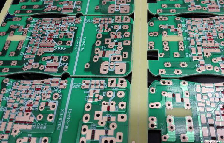
On the SMT line, if the PCB board is not flat, it will cause inaccurate positioning, components cannot be inserted or mounted on the holes and surface mount pads of the PCB board, and the automatic insertion machine may even be damaged. The PCB board with the components is bent after soldering, and the component feet are difficult to cut neatly. The PCB board cannot be installed on the chassis or the socket in the machine, so it is also very annoying for the assembly plant to encounter the board warping. The current surface mount technology is developing in the direction of high, high speed and intelligence, which puts forward higher flatness requirements for the PCB board as the home of various components.
In the IPC standard, it is specifically pointed out that the allowable bow and twist amount for PCB boards with surface mount devices is 0.75%, and the allowable bow and twist amount for PCB boards without surface mount devices is 1.5%. In fact, in order to meet the needs of high and high-speed placement, some electronic assembly manufacturers have stricter requirements on the amount of PCB bow and twist. For example, ipcb has many customers who require a PCB bow and twist amount of 0.5%, or even Some customers require 0.3%.

PCB bow and twis
PCB board is composed of copper foil, resin, glass cloth and other materials. The physical and chemical properties of each material are different. After being pressed together, thermal stress will inevitably occur, resulting in PCB bow and twist. At the same time, in the PCB board processing process, it will go through various processes such as high temperature, mechanical cutting, wet treatment, etc., which will also have an important impact on the deformation of the board. In short, the reasons for the deformation of the PCB board can be complicated and diverse. How to reduce or eliminate the material Different characteristics or deformation caused by processing have become one of the complex problems faced by PCB board manufacturers.
The bow and twist of PCB board needs to be researched from several aspects such as material, structure, pattern distribution, processing process, etc. ipcb will analyze and explain various reasons and improvement methods that may cause deformation.
The area of the copper surface on the PCB board is uneven, which will worsen the bending and warping of the board.
Generally, a large area of copper foil is designed on the PCB board for grounding purposes. Sometimes there is also a large area of copper foil designed on the Vcc layer. When these large area copper foils cannot be evenly distributed on the same PCB board When it is installed, it will cause the problem of uneven heat absorption and heat dissipation. Of course, the PCB board will also expand and contract. If the expansion and contraction cannot be done at the same time, it will cause different stress and deformation. At this time, if the PCB temperature has reached At the upper limit of the Tg value, the board will begin to soften, causing deformation.
The connection points (vias, vias) of each layer on the PCB board will limit the expansion and contraction of the PCB.
Today's PCB boards are mostly multi-layer boards, and there will be rivet-like connection points (vias) between the layers. The connection points are divided into through holes, blind holes and buried holes. Where there are connection points, the board will be restricted. The effect of expansion and contraction will also indirectly cause PCB bow and twist.