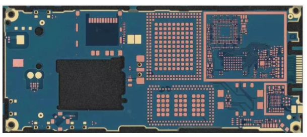
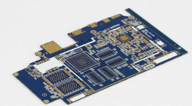
In order to meet the urgent requirements of the electronics industry for the ban on lead, the printed circuit board industry is shifting the final surface treatment from hot-air leveling tin spray (tin-lead eutectic) to other surface treatments, including organic protective film (OSP), Immersion Silver, Immersion Tin and Chemical Nickel Immersion Gold. OSP film is considered to be the best choice due to its excellent solderability, simple process and low operating cost.
In this paper, thermal desorption-gas chromatography-mass spectrometry (TD-GC-MS), thermogravimetric analysis (TGA) and photoelectron spectroscopy (XPS) are used to analyze the heat resistance characteristics of a new generation of high temperature resistant OSP films. Gas chromatography tests the small molecular organic components in the high temperature resistant OSP film (HTOSP) that affect the solderability, and at the same time shows that the alkylbenzimidazole-HT in the high temperature resistant OSP film has very little volatility. The TGA data shows that the HTOSP film has a higher degradation temperature than the current industry standard OSP film. XPS data shows that after 5 lead-free reflows of high-temperature OSP, the oxygen content only increased by about 1%. The above improvements are directly related to the requirements of industrial lead-free solderability.
OSP film has been used in circuit boards for many years. It is an organometallic polymer film formed by the reaction of azole compounds with transition metal elements, such as copper and zinc. Many studies have revealed the corrosion inhibition mechanism of azole compounds on metal surfaces. G.P.Brown successfully synthesized benzimidazole, copper (II), zinc (II) and other transition metal elements of organometallic polymers, and described the excellent high temperature resistance of poly(benzimidazole-zinc) through TGA. G.P.Brown’s TGA data shows that the degradation temperature of poly(benzimidazole-zinc) is as high as 400°C in the air and 500°C in a nitrogen atmosphere, while the degradation temperature of poly(benzimidazole-copper) is only 250°C. The recently developed new HTOSP film is based on the chemical properties of poly(benzimidazole-zinc), which has the best heat resistance.

OSP film is mainly composed of organometallic polymers and small organic molecules entrained during the deposition process, such as fatty acids and azole compounds. Organometallic polymers provide the necessary corrosion resistance, copper surface adhesion, and surface hardness of OSP. The degradation temperature of the organometallic polymer must be higher than the melting point of the lead-free solder to withstand the lead-free process of PCB copying. Otherwise, the OSP film will be degraded after being processed by the PCB copy board lead-free process. The degradation temperature of the OSP film largely depends on the heat resistance of the organometallic polymer. Another important factor that affects the oxidation resistance of copper is the volatility of azole compounds, such as benzimidazole and phenylimidazole. The small molecules of the OSP film will evaporate during the lead-free reflow process, which will affect the oxidation resistance of copper. Gas chromatography-mass spectrometry (GC-MS), thermogravimetric analysis (TGA), and photoelectron spectroscopy (XPS) can be used to scientifically explain the heat resistance of OSP.
experiment
1. Gas chromatography-mass spectrometry analysis
The copper plates tested were coated with: a) a new HTOSP film; b) an industry standard OSP film; and c) another industrial OSP film. Scrape about 0.74-0.79 mg of OSP film from the copper plate. These coated copper plates and the scraped samples have not undergone any reflow treatment. This experiment uses H/P6890GC/MS instrument, and uses syringe without syringe. Syringe-free syringes can directly desorb solid samples in the sample chamber. The syringe without syringe can transfer the sample in the small glass tube to the inlet of the gas chromatograph. The carrier gas can continuously bring the volatile organic compounds to the gas chromatograph column for collection and separation. Place the PCB sample close to the top of the column so that thermal desorption can be effectively repeated. After enough samples were desorbed, the gas chromatography started to work. In this experiment, a RestekRT-1 (0.25mmid*30m, film thickness of 1.0μm) gas chromatography column was used. The temperature rise program of the gas chromatography column: After heating at 35°C for 2 minutes, the temperature starts to rise to 325°C, and the heating rate is 15°C/min. The thermal desorption conditions are: after heating at 250°C for 2 minutes. The mass/charge ratio of the separated volatile organic compounds is detected by mass spectrometry in the range of 10-700daltons. The retention time of all small organic molecules is also recorded.
2. Thermogravimetric analysis (TGA)
Similarly, a new HTOSP film, an industry standard OSP film, and another industrial OSP film were coated on the samples. Approximately 17.0 mg of OSP film was scraped from the copper plate as a material test sample. Before the TGA test, neither the sample nor the film can undergo any lead-free reflow treatment. Use TA Instruments' 2950TA to perform TGA test under nitrogen protection. The working temperature was kept at room temperature for 15 minutes, and then increased to 700°C at a rate of 10°C/min.
3. Photoelectron spectroscopy (XPS)
Photoelectron Spectroscopy (XPS), also called Chemical Analysis Electron Spectroscopy (ESCA), is a chemical surface analysis method. XPS can measure the 10nm chemical composition of the coating surface. Coat the HTOSP film and industry standard OSP film on the copper plate, and then go through 5 lead-free reflows. XPS was used to analyze the HTOSP film before and after the reflow treatment. The industry-standard OSP film after 5 lead-free reflow was also analyzed by XPS. The instrument used was VGESCALABMarkII.
4. PCB through hole solderability test
Using solderability test boards (STVs) for through-hole solderability testing. There are a total of 10 solderability test board STV arrays (each array has 4 STVs) coated with a film thickness of about 0.35μm, of which 5 STV arrays are coated with HTOSP film, and the other 5 STV arrays are coated with industry standard OSP film. Then, the coated STVs undergo a series of high-temperature, lead-free reflow treatments in the solder paste reflow oven. Each test condition includes 0, 1, 3, 5 or 7 consecutive reflows. There are 4 STVs for each type of film for each reflow test condition. After the reflow process, all STVs are processed for high temperature and lead-free wave soldering. Through-hole solderability can be determined by inspecting each STV and calculating the number of correctly filled through-holes. The acceptance criterion for through holes is that the filled solder must be filled to the top of the plated through hole or the upper edge of the through hole.
Each STV has 1196 through holes
10milholes-Fourgrids,100holeseachgridsquareandrou ndpads
20milholes-Fourgrids,100holeseachgridsquareandrou ndpads
30milholes-Fourgrids,100holeseachgridsquareandrou ndpads
5. Test the solderability through a tin-dip balance
The solderability of the OSP film can also be determined by the dip-tin balance test. Coat the HTOS P film on the test panel of the dipped tin balance, after 7 times of lead-free reflow, Tpeak=262 degree Celsius. Use BTUTRS combined with IR/convection reflow oven for reflow treatment in the air. Conduct wet-tin balance test in accordance with IPC/EIAJ-STD-003A section 4.3.1.4, using "RoboticProcessSystems" automated wet-tin balance tester, EF-8000 flux, non-clean flux and SAC305 alloy solder.
6. PCB solder bonding force test
PCB welding bonding force can be measured by shearing force. Coat the HTOSP film on the BGA pad test board (diameter 0.76mm), the thickness of which is 0.25 and 0.48μm respectively, and undergoes three lead-free reflow treatments with a maximum temperature of 262°C. And use matching solder paste to solder to the pad, the solder ball is SAC305 alloy (diameter 0.76mm). The shear test was carried out with a DagePC-400 adhesion tester at a shear speed of 200μm/see.