1. The FR-4 we often choose is not a material name
The "FR-4" often referred to by circuit board factories is a code name for the grade of flame retardant materials. It represents a material specification that the resin material must be able to extinguish itself after being burned. It is not a material name, but A material grade, so there are many types of FR-4 grade materials used in general circuit boards, but most of them are based on the so-called tera-function epoxy resin plus filler and filler. Composite material made of glass fiber.
For example, the FR-4 water-green fiberglass board and black fiberglass board that our family makes now have the functions of high temperature resistance, insulation, and flame retardant. So when choosing materials, everyone must figure out what characteristics they need to achieve. In this way, you can buy the products you need.
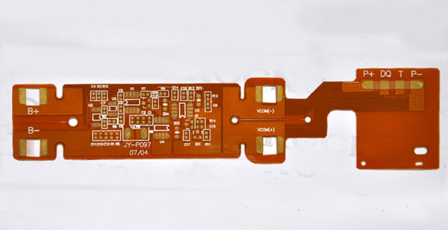
Flexible printed circuit board (Flexible Printed Circuit Board, abbreviated FPC) is also called flexible printed circuit board, or flexible printed circuit board. The flexible printed circuit board is a product that is designed and manufactured on a flexible substrate by means of printing.
There are two main types of printed circuit board substrates: organic substrate materials and inorganic substrate materials, and organic substrate materials are the most used. The PCB substrates used for different layers are also different. For example, prefabricated composite materials are used for 3- to 4-layer boards, and glass-epoxy materials are mostly used for double-sided boards.
2. When choosing a sheet, we need to consider the impact of SMT
In the process of lead-free electronic assembly, as the temperature rises, the degree of bending of the printed circuit board when heated is increased. Therefore, it is required to use a board with a small degree of bending in SMT, such as FR-4 type substrate. Since the expansion and contraction stress of the substrate after heating affects the component, it will cause the electrode to peel off and reduce the reliability, so you should also pay attention to the material expansion coefficient when selecting the material, especially when the component is larger than 3.2*1.6mm.
The PCB used in surface assembly technology requires high thermal conductivity, excellent heat resistance (150 degree Celsius, 60min) and solderability (260 degree Celsius, 10s), high copper foil adhesion strength (1.5*104Pa or more) and bending strength (25 *104Pa), high conductivity and small dielectric constant, good punchability (accuracy ±0.02mm) and compatibility with cleaning agents, in addition, the appearance is required to be smooth and flat, without warpage, cracks, scars, and rust spots.
3. PCB thickness selection

The thickness of the printed circuit board is 0.5mm, 0.7mm, 0.8mm, 1mm, 1.5mm, 1.6mm, (1.8mm), 2.7mm, (3.0mm), 3.2mm, 4.0mm, 6.4mm, of which 0.7mm and 1.5 The PCB of mm board thickness is used for the design of double-sided board with gold fingers, and 1.8mm and 3.0mm are non-standard sizes. From the perspective of production, the size of the printed circuit board should not be smaller than 250*200mm, and the ideal size is generally (250~350mm)*(200*250mm). For PCBs with long sides less than 125mm or wide sides less than 100mm, Using jigsaw method. The surface mount technology stipulates the bending amount of the substrate with a thickness of 1.6mm as upper warpage ≤0.5mm and lower warpage ≤1.2mm.
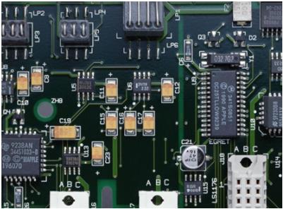
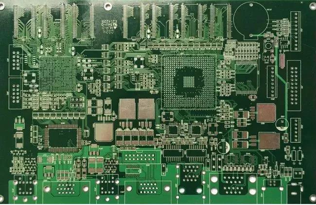
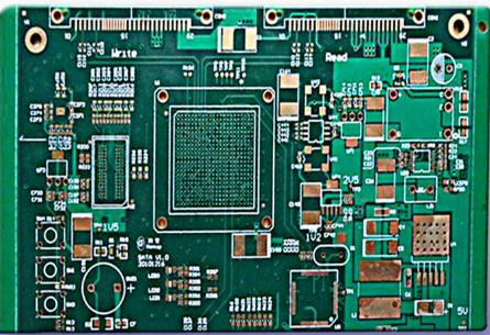
Generally, the allowable bending rate is below 0.065%. It is divided into 3 types according to metal materials, as shown in typical PCBs; 3 types according to structural softness and hardness. Electronic plug-ins are also developing towards high pin count, miniaturization, SMD and complexity. . The electronic plug-in is installed on the circuit board through the pins and the pins are soldered on the other side. This technology is called THT (Through Hole Technology) plug-in technology. In this way, a hole must be drilled for each pin on the PCB, which shows the typical application of PCB.
4. Drilling
With the rapid development of SMT chip technology, multi-layer circuit boards need to be connected to each other, which is guaranteed by electroplating after drilling, which requires various drilling equipment. In order to meet the above requirements, at present, PCB CNC drilling equipment with different performance is launched at home and abroad.
The production process of printed circuit boards is a complex process. It involves a wide range of processes, mainly involving photochemistry, electrochemistry, and thermochemistry; there are also many process steps involved in the PCB production process, with hard Multi-layer circuit boards are taken as an example to illustrate the processing procedures.