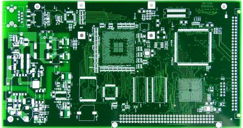
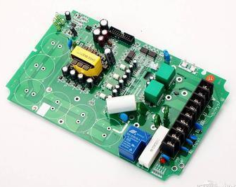
With the increase in circuit density and the elimination of product form factors, many new methods have emerged in the PCB industry to integrate chip-level design more closely with board-level assembly. To a certain extent, the emergence of technologies such as flip chip and chip scale package (CSP) has actually blurred the semiconductor die, chip packaging method and printed circuit board (PCB). ) The traditional dividing line between assembly-level craftsmanship. Although the advantages of these new high-density chip-level assembly technologies are very important, as smaller sizes make components, connections, and packaging more sensitive to physical and temperature stress, choose the best technology to configure and achieve continuous reliability. The production effect becomes more and more difficult.
1. Why is it filled?
The initial idea of considering the use of underfill sealant is to reduce the impact caused by the mismatch of the overall temperature expansion characteristics between the silicon die and the underlying substrate to which it is attached.
The second benefit of glue filling is to prevent moisture and other forms of pollution. On the negative side, the use of filler increases the cost of manufacturing operations and makes rework difficult. Because of this, many PCBA manufacturers perform quick functional tests after reflow and before filling.
Second, decide when to fill the glue

Because there are no less than fifty different CSP designs1, plus countless variables and operating conditions involving connection design, it is difficult to provide an exact rule to determine when to use filling. However, there are many key factors that should be taken into consideration when designing a PCB. Some important factors include:
The difference in the coefficient of temperature expansion (CTE) between the chip and the substrate. The CTE of silicon is 2.4 ppm; the CTE of a typical PCB material is 16 ppm. Ceramic materials can be designed according to the matching CTE, but the CTE of 95% alumina ceramics is 6.3 ppm. Adhesive filling is required for PCB-based packaging, although the increased reliability after filling is also shown on ceramic substrates. An alternative method is to use a substrate with an insert structure, such as a high-CTE ceramic or flexible material, as a vibration-absorbing material between the chip and the main substrate, which can reduce the CTE difference between the PCB and the silicon chip.
Fourth, the system PCB thickness
Experience has shown that thicker PCBs are more rigid, and thinner boards resist bending forces caused by greater impact. For example, an analysis proved that increasing the thickness of the FR-4 substrate from 0.6mm to 1.6mm can increase the number of cycles-to-failure tests from 600 to 9003. Unfortunately, for today's ultra-small devices, increasing the thickness of the substrate is always unrealistic. In fact, every doubling of the substrate thickness increases the reliability improvement by approximately two times, but the doubling of the chip size causes a four-fold degradation4.
Five, the challenge of Dijiao
Once the decision to use the filling method is made, a series of challenges must be considered in order to effectively implement the process and obtain continuous and reliable results while maintaining the required production level. These key issues include:
Obtain complete and void-free glue flow at the bottom of the chip
Distribute glue around tightly packed chips
Avoid contamination of other components
Dispensing glue through the opening of the radio frequency (RF) housing or shield
Control flux residues.
6. Obtain a complete and void-free glue flow
Because the filling material must be sucked into the bottom of the chip by capillary action, the key is to place the needle close enough to the chip to start the flow of glue. Care must be taken to avoid touching the chip or contaminating the back of the die. A recommended principle is to position the starting point of the needle tip at half the outer diameter of the needle tip plus a 0.007" XY displacement. The height of Z is 80% of the height of the chip on the substrate. During the entire dispensing process, Precision control is also required to maintain the flow of the glue, and avoid damage and contamination of the die.
Seven, the number of chips and the neighbor relationship
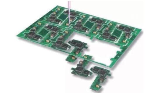
When designing a tightly packed die on a board that needs to be filled with glue at the bottom, the board designer needs to leave enough space for the glue nozzle. Two chips sharing a glue route is an acceptable glue dispensing method. Passive components parallel to the edge of the chip will have a blocking effect. Components at 90° to the edge of the chip may attract glue away from the component to be filled. The filling material around the passive components has not been found to have a bad effect. Cross capillary action from adjacent chips or passive components will attract the filling material away from the target components, which may cause voids under the CSP or flip chip
8. Eject glue through the opening
With the increase in the use of underfill in RF assembly, it is often necessary to challenge the glue dispensing process and implement the glue filling process after the RF shielding cover has been assembled. For the best production efficiency, it is usually necessary to consider positioning the RF shielding cover while other components are mounted, and solder everything in a one-time reflow soldering process. Therefore, product and process designers must cooperate to leave enough openings in the shield cover for the bottom filling. The designer must also avoid placing the chip too close to the RF shielding cover, because capillary action or high-speed dispensing may allow the filling material to flow into the RF shielding cover and above the CSP or flip chip. If the gap between the component and the cover is small, the speed of dripping the filling material will be limited to avoid filling on the component. Slowing down the dispensing rate will slow down the assembly process and limit output. Move to another hole or component, and then return to the first hole to drop more glue, which may shift a little. However, this involves multiple movements, once again reducing output.
Schwiebert and Leong gave an equation for the flow rate of filling glue.
The flow time is:
t = 3 μL2/[h λcos(φ)]
here:
T = time (seconds)
Μ = fluid viscosity
L = travel distance
H = clearance or ball height
Φ = contact or wetting angle
Λ = surface tension at the liquid-vapor interface
(The values of these parameters need to be obtained at the liquid dispensing temperature, usually 90°C.)
Pumps and valves from most PCBA manufacturers can deliver liquid to the CSP or flip chip faster than the material can flow under the chip. The volume/weight of the liquid under the chip still needs to be determined8. Once these numbers are determined, the first approximate calculation of the flow rate is made to determine whether the liquid should be dropped at one time or a small amount of multiple drops. The typical process is: when the liquid is flowing under the first component, move to the second component to drop glue, and then return to the first position to complete.
11. Conclusion
The effective use of glue filling requires a wide range of factors including the design of PCB products to adapt to the glue filling process and the design of glue filling technology to adapt to product needs. Accurate and flexible filling of glue for chip-level design requirements will inevitably involve the partnership between product designers, manufacturing process engineers, glue preparers, and glue system suppliers.