When some PCB prototype manufacturers promote their products, they will specifically mention that their products use special processes such as gold plating and silver plating. So what is the use of this process?
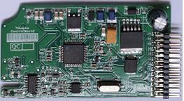
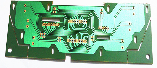
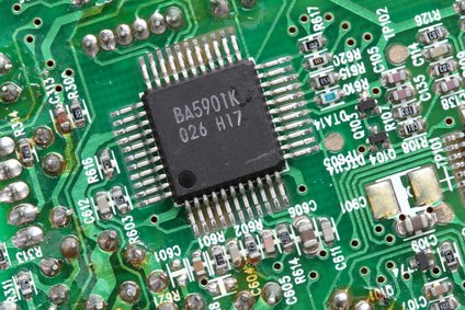
The surface of the PCB prototype requires soldering components, so a part of the copper layer is required to be exposed for soldering. These exposed copper layers are called pads. The pads are generally rectangular or round with a small area. We know that the copper used in the PCB prototype is easily oxidized, so after applying the solder mask, the copper on the pad is exposed to the air.
If the copper on the pad is oxidized, it is not only difficult to solder, but also the resistivity greatly increases, which seriously affects the performance of the final product. Therefore, engineers came up with various methods to protect the pads. For example, it is plated with inert metal gold, or the surface is covered with a layer of silver through a chemical process, or a special chemical film is used to cover the copper layer to prevent contact between the pad and the air.

PCB prototype gold plating and silver plating
For the exposed pads on the PCB prototype, the copper layer is directly exposed. This part needs to be protected to prevent it from being oxidized. From this point of view, whether it is gold or silver, the purpose of the process itself is to prevent oxidation and protect the pad, so that it can ensure the yield in the subsequent soldering process.
However, the use of different metals will impose requirements on the storage time and storage conditions of the PCB prototype used in the production plant. Therefore, the PCB prototype factory will usually use the vacuum plastic packaging machine to package the PCB prototype before the PCB prototype is produced and delivered to the customer to ensure that the PCB prototype does not suffer from oxidation damage.
Before the components are welded on the machine, the board manufacturer must also check the oxidation degree of the PCB prototype, and eliminate the oxidation PCB prototype to ensure the yield. The boards received by the end consumers have undergone various tests, even if they are used for a long time, the oxidation will almost only occur at the plug-in connection parts, and has no effect on the soldering pads and already soldered components.
Since the resistance of silver and gold is lower, will the use of special metals such as silver and gold reduce the heat generated when the PCB prototype is used?
We know that the factor that affects the amount of heat is resistance. The resistance is related to the material of the conductor itself, the cross-sectional area and length of the conductor. The thickness of the metal material on the surface of the pad is even far less than 0.01 mm. If the pad is processed by the OST (organic protective film) method, there will be no excess thickness at all. The resistance exhibited by such a small thickness is almost equal to 0, even impossible to calculate, and of course it will not affect the heat generation.