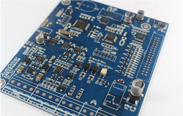
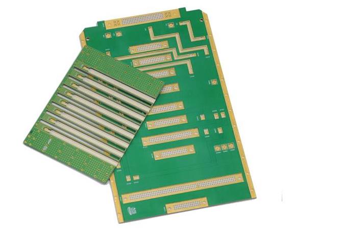
Hot air leveling
Hot air leveling is a process of coating molten tin-lead solder on the surface of the PCB and leveling (flattening) with heated compressed air to form a coating layer that is resistant to copper oxidation and provides good solderability. During hot air leveling, the solder and copper form a copper-tin metal compound at the junction, and its thickness is about 1 to 2 mils.
Advantages: low cost
shortcoming:
1. The pads processed by HASL technology are not flat enough, and the coplanarity cannot meet the process requirements of fine-pitch pads.
2. It is not environmentally friendly, and lead is harmful to the environment.
Four, gold-plated board

Gold plating uses real gold, even if it is only plated with a thin layer, it already accounts for nearly 10% of the cost of the circuit board. Use gold as a plating layer, one is to facilitate welding, and the other is to prevent corrosion. Even the golden finger of the memory stick that has been used for several years is still shiny as before.
Advantages: strong conductivity and good oxidation resistance. The coating is dense and wear-resistant, and is generally used in bonding, welding and plugging.
Disadvantages: higher cost and poor welding strength.
Five, chemical gold/immersion gold
Chemical nickel immersion gold, also called chemical nickel gold, immersion nickel gold, abbreviated chemical gold and immersion gold. Gold is chemically coated on the copper surface with a thick layer of nickel-gold alloy with good electrical properties and can protect the PCB for a long time. The deposition thickness of the inner layer of nickel is generally 120~240μin (about 3~6μm), and the deposition thickness of the outer layer of gold is generally 2~4μinch (0.05~0.1μm).
advantage:
1. The surface of the PCB treated with gold is very flat and has good coplanarity, which is suitable for the contact surface of the button.
2. The solderability of chemical gold is excellent, gold will quickly melt into the molten solder, and the solder and Ni form a Ni/Sn metal compound.
Disadvantages: The process is complicated, and it is necessary to strictly control the process parameters to achieve good results. The most troublesome thing is that the gold-treated PCB surface is prone to black plate benefits during ENIG or soldering. It is directly manifested as excessive oxidation of Ni and too much gold, which will embrittle solder joints and affect reliability.
Six, electroless nickel palladium plating
Electroless nickel and palladium add a layer of palladium between nickel and gold. During the deposition reaction of replacement gold, the electroless palladium layer protects the nickel layer from excessive corrosion by the replacement gold. Palladium prevents corrosion caused by the replacement reaction. At the same time, make full preparations for immersion gold. The deposition thickness of nickel is generally 120~240μin (about 3~6μm), and the thickness of palladium is 4~20μin (about 0.1~0.5μm). The deposition thickness of gold is generally 1~4μin (0.02~0.1μm).
Advantages: It has a very wide range of applications. At the same time, the chemical nickel-palladium-gold surface treatment can effectively prevent the connection reliability problems caused by the black pad defect and can replace the nickel-gold surface treatment.
Disadvantages: Although ENEPIG has many advantages, palladium is expensive and it is a scarce resource. At the same time, it has strict process control requirements, just like nickel gold.
Seven, spray tin circuit board
The silver board is called the spray tin board. Spraying a layer of tin on the outer layer of the copper circuit can also help soldering. But it cannot provide long-term contact reliability like gold. Basically used as the circuit board of small digital products, without exception, the spray tin board, the reason is that it is cheap.
Advantages: lower price, good welding performance.
Disadvantages: Not suitable for welding pins with fine gaps and components that are too small, because the surface flatness of the spray tin plate is poor. Tin beads are prone to be produced in PCB processing, and it is easier to cause short circuits to the components of the fine-gap pins.