With the emergence of new semi-additive technologies on printed circuit boards (PCBs), the trace width can be reduced by half to 1.25 mils. Therefore, the circuit assembly density can be maximized. According to a report on the EETimes website, the current continuous advancement of integrated circuits has shifted from the semiconductor IC lithography process (Lithography) to the PCB process in the past.
At present, the most commonly used subtractive PCB process in the PCB industry, the minimum tolerance of the wiring design width can be within 0.5 mil. Analysts pointed out that for those with a wiring design width of more than 3mils and a relatively low signal edge rate, although the 0.5mil change value is not obvious, it has a significant impact on the impedance control of the thinner wiring design.
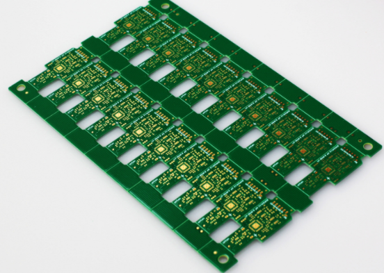
First, the PCB manufacturing process basically covers one or both sides with a copper-containing substrate material, which is the so-called core. Each PCB manufacturer uses a different copper substrate material and thickness on the substrate, so the insulation and mechanical characteristics are also different.
Then, after pressing the copper foil and the substrate material to form a substrate, the substrate is covered with an anti-corrosion agent before exposure,

and then the unexposed anti-corrosion agent and copper are etched in an acid bath to form a wiring design. The purpose of this approach is to allow the wiring design to form a rectangular section, but during the acid bath process, not only the vertical copper will be eroded, but also part of the horizontal wiring design wall will be dissolved.
The subtractive method under strict control can make the wiring design form a trapezoidal cross-section of almost 25 to 45 degrees. However, if it is not properly controlled, it will cause the upper half of the wiring design to be over-etched, resulting in a narrow top and thick bottom. . If the height of the etched wiring design is compared with the etched depth of the upper half of the wiring design, the so-called etch factor will be obtained. The larger the value, the more rectangular the wiring design section is.
Once the wiring design can be rectangular, it means that its impedance (Impedance) is more predictable, and it can be repeated almost vertically, which means that the circuit assembly density can reach the highest. From the perspective of signal integrity, PCB manufacturing yield can also be improved.
The same method that can achieve this result is semi-additive. The substrate of this method is laminated with a copper foil with a thickness of 2 or 3 microns (μm) thinner, and then the via hole is drilled and covered with electroless copper.
Then, an anti-corrosion agent is added in a specific range for exposure to form the required wiring design. After the exposed areas are stacked, the remaining copper is etched. Therefore, this method is basically the opposite of the subtractive method. Compared with the chemical principle of the subtractive method, the wiring design of the partial additive method basically uses Photolithography. Therefore, the width of the wiring design formed by the latter is more in line with the original design.
Under extremely strict tolerances, its wiring design width can maintain a level of 1.25 mils and have a certain level of impedance control. It is found through actual measurement that the impedance change measured on the entire PCB board will not exceed 0.5 ohm, which is one-fifth of the subtraction method.
The analysis pointed out that accurate impedance control is indispensable to meet the requirements of high-speed digital systems and microwave applications, which can also be achieved through partial additive methods. Moreover, it can achieve almost vertical wiring design characteristics, which can maximize the circuit assembly density.