DFM (Design for manufacturability) is design for manufacturing, and it is the core technology of concurrent engineering. Design and manufacturing are the two most important links in the product life cycle. Concurrent engineering is to consider factors such as product manufacturability and assemblability at the beginning of the design. So DFM is the most important support tool in concurrent engineering. Its key is the processability analysis of design information, the evaluation of manufacturing rationality and the suggestions for improving the design. In this article, we will briefly introduce the DFM general technical requirements in the PCB process.
1. General requirements
1. As a general requirement for PCB design, this standard regulates PCB design and manufacturing and realizes effective communication between CAD and CAM.
2. PCB company prioritizes design drawings and documents as production basis when processing documents.
2. PCB material
1. Substrate
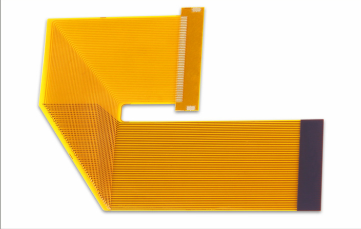
The substrate of PCB generally adopts epoxy glass cloth copper clad laminate, namely FR4. (Including single panel)
2. Copper foil
a) More than 99.9% electrolytic copper;
b) The thickness of copper foil on the surface of the finished double-layer board is ≥35?m (1OZ); when there are special requirements, specify in the drawings or documents.

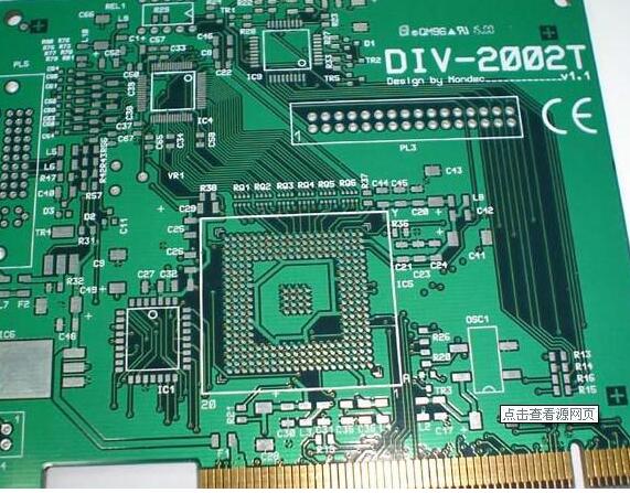
3. PCB structure, dimensions and tolerances
1. Structure
a) All relevant design elements that make up the PCB should be described in the design drawings. The appearance should be uniformly represented by Mechanical 1 layer (priority) or Keep out layer. If it is used in the design file at the same time, generally keep out layer is used for shielding, without opening holes, and using mechanical 1 for forming.
b) In the design drawing, it means to open a long slot hole or hollow out, and use the Mechanical 1 layer to draw the corresponding shape.
2. Board thickness tolerance
3. Overall dimension tolerance
The external dimensions of the PCB should conform to the requirements of the design drawings. When the drawing is not specified, the tolerance of the external dimension is ±0.2mm. (Except for V-CUT products)
4. Flatness (warpage) tolerance
The flatness of the PCB should meet the requirements of the design drawings.
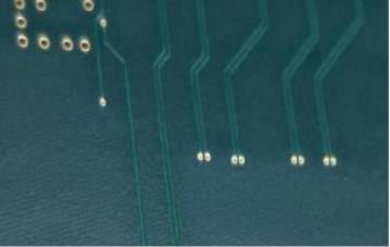
Four, printed wires and pads
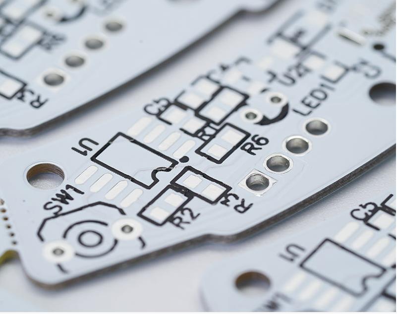
1. Layout
a) In principle, the layout, line width and line spacing of printed wires and pads shall be in accordance with the design drawings. However, our company will deal with the following: appropriately compensate the line width and PAD ring width according to the process requirements. In general, our company will try to increase the PAD as much as possible for the single panel to enhance the reliability of customer welding.
b) When the design line spacing does not meet the process requirements (too dense may affect performance and manufacturability), our company will make appropriate adjustments according to the pre-manufacturing design specifications.
c) In principle, our company recommends that when customers design single and double panels, the inner diameter of the via (VIA) should be set to 0.3mm or more, the outer diameter to be set to 0.7mm or more, the line spacing design is 8mil, and the line width design is 8mil or more. In order to reduce the production cycle to the greatest extent, reduce the manufacturing difficulty.
d) The minimum drilling tool of our company is 0.3, and the finished hole is about 0.15mm. The minimum line spacing is 6mil. The thinnest line width is 6mil. (But the manufacturing cycle is longer and the cost is higher)
2. Wire width tolerance
The internal control standard for the width tolerance of printed wires is ±15%
3. Grid processing
a) In order to avoid blistering on the copper surface during wave soldering and PCB bending due to thermal stress after heating, it is recommended to lay the large copper surface in a grid pattern.
b) The grid spacing is greater than or equal to 10mil (not less than 8mil), and the grid line width is greater than or equal to 10mil (not less than 8mil).
4. Treatment of thermal pad
In large-area grounding (electricity), the legs of components are often connected to it. The treatment of the connecting legs takes into account the electrical performance and process requirements. The possibility of excessively dispersing heat and producing virtual solder joints is greatly reduced.
5. Aperture (HOLE)
1. Definition of metallization (PHT) and non-metallization (NPTH)
a) Our company defaults the following methods as non-metallized holes:
When the customer sets the non-metallized properties of the mounting holes in the advanced properties of Protel99se (remove the plated item in the Advanced menu), our company defaults to non-metallized holes.
When the customer directly uses keep out layer or mechanical 1-layer arc in the design file to indicate the hole punching (there is no separate hole), our company defaults to non-metalized holes.
When the customer places NPTH near the hole, our company defaults that the hole is non-metallized.
When the customer clearly requires the corresponding aperture non-metallization (NPTH) in the design notice, it will be handled as required by the customer.
b) All component holes, mounting holes, via holes, etc. other than the above should be metallized.
2. Aperture size and tolerance
a) The PCB component holes and mounting holes in the design drawings default to the final finished aperture size. The tolerance of the aperture is generally ±3mil (0.08mm);
b) The via hole (ie VIA hole) is generally controlled by our company: negative tolerance is not required, and positive tolerance is controlled within + 3mil (0.08mm).
3. Thickness
The average thickness of the copper-plated layer of metallized holes is generally not less than 20 m, and the thinnest part is not less than 18 m.
4. Hole wall roughness
PTH hole wall roughness is generally controlled within ≤ 32um
5. PIN hole problem
a) The minimum positioning pin of the CNC milling machine of PCB company is 0.9mm, and the three pin holes for positioning should be triangular.
b) When the customer has no special requirements, and the aperture in the design documents is less than 0.9mm, our company will add PIN holes at the appropriate positions on the blank wireless road or the large copper surface in the board.
6. SLOT hole (slot hole) design
a) It is recommended to use Mechanical 1 layer (Keep out layer) to draw the shape of the slot hole; it can also be represented by a connecting hole, but the connecting hole should be of the same size and the center of the hole should be on the same horizontal line.
b) Our smallest slot cutter is 0.65mm.
c) When opening the SLOT hole for shielding to avoid creepage between high and low voltages, it is recommended that its diameter be above 1.2mm to facilitate processing.
Six, solder mask
1. Coating parts and defects
a) All PCB surfaces except for pads, MARK points, test points, etc. should be coated with solder mask.
b) If the customer uses the disk represented by FILL or TRACK, the corresponding size graphics must be drawn on the solder mask layer to indicate that the place is tinned. (Our company strongly recommends not to display disks in non-PAD format before designing)
c) If you need to dissipate heat on the large copper skin or spray tin on the lines, you must also draw a corresponding size figure with a solder mask layer to indicate the place where tin is applied.
2. Adhesion
The adhesion of the solder mask is in accordance with the Class 2 requirements of the US IPC-A-600F.
Seven, concluding remarks
The above DFM general technical requirements (single and double panel part) are only for customers' reference when designing PCB files, and hope to negotiate and reconcile the above aspects, so as to better realize the communication between CAD and CAM, and achieve better The common goal of Design for Manufacturability (DFM) is to shorten the product manufacturing cycle and reduce production costs.