In recent years, smartphones and tablets have become important product items that drive the continuous optimization of computer technology. Not only do products become thinner and lighter, their functions are undiminished, and even their performance, storage capacity, and product battery life can double or even multiply each time. In addition to the integrated effect of semiconductor technology in 3D IC and high-end heterogeneous packaging technology, the other is the upgrade of PCB carrier technology capabilities in response to the challenges of new components and smaller size and narrower internal space. .
Circuit boards have a huge impact on the electronics industry
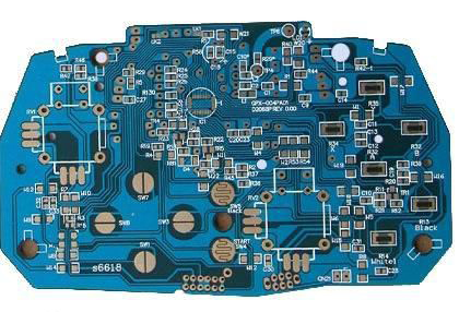
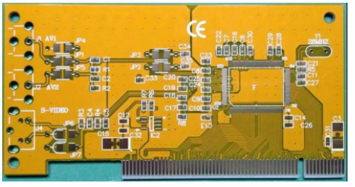
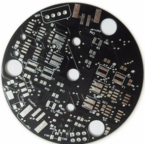
The printed circuit board (PCB) plays a key role in carrying a large number of electronic components and constructing component conduction circuits. PCB has also become an important component for the continuous evolution and upgrading of electronic products! PCB circuit production is mainly divided into two methods. Basically, the PCB itself must have an insulating carrier board. The material of the carrier board determines the strength, insulation effect and basic electrical performance of the PCB circuit board itself, and the conduction line can be added Constructed in two different production methods: Additive or Subtractive.
Soft board? Different advantages of hard board use conditions
The circuit addition method is made by metal plating, vapor deposition or conductive material addition of the physical circuit on the substrate; the subtraction method is to adopt the printed circuit pattern on the substrate that has been covered with the metal conductor layer. The metal of the non-printed wireless circuit block is corroded and removed by a chemical solvent to form a circuit.

From single-layer to double-layer or even multi-layer, testing the precision of manufacturing and chemical processing
Generally, the conductive layer (circuit) structure of the base material can be set on the upper and lower sides of the substrate, and the connecting and conductive lines of the upper and lower circuit lines are formed by drilling and plating through the lines in the hole. With the electronic product industry The demand for high-precision and high-complexity integrated circuits has also resulted in the stacking of multiple rigid circuit boards, and the design of conduction connections and bonding between circuit layers and layers to build a more complex multi-layer board structure.
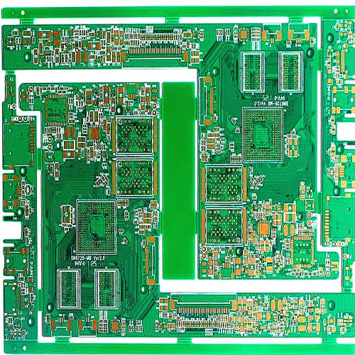
Multi-layer PCB can effectively simplify the size and area of the substrate. Especially with the highly integrated components of IC technology, the circuit carrier can even reduce the spectrum of traditional circuits by several to tens of times, which has become a key design trend for electronic products to actively shrink and optimize.
The integrated design of multi-layer boards and high-density PCBs is not only much higher in product technology than conventional circuit boards, but also more profit in products than conventional products, but there are relatively more problems that follow.
Therefore, although high-density multilayer boards have the advantages of high profits and high material accumulation and reduction, the derived testing and verification work will be more complicated and more demanding. The precision and material temperature change also need to pass through the substrate material. Optimizing and providing high stability and resistance to temperature changes can enable the terminal electronic products to better meet the design requirements.
The choice of metal layer material affects the electrical properties of the circuit
In addition to the material properties of the substrate, the metal layer placed on the substrate is also the key to the overall performance of the circuit board.
The current circuit board is mainly composed of circuit and pattern. Generally, the circuit and the pattern are made together, and the insulating board of the base material itself establishes the insulating electrical properties of each layer (dielectric layer (Dielectric)). Each layer of the carrier board is used to form application circuit connections through through holes/vias. Generally speaking, larger through holes are for electronic components that need to be plug-in soldered, and the circuit board will also be non-conductive. Hole for setting and soldering of surface-mounted electronic components.
Finishing process with plate processing to improve the stability and durability of the circuit board
The composite board itself, if the air is humid, will easily cause the board to mutate and deform due to the absorption of moisture, and the deformation process may cause the line conductor to break or contact poorly. In order to increase the life of the board, a layer of epoxy resin is usually added to the unwelded surface of the board or the surface of the board, or with reference information such as the name and location of the silk-printed component, the version number of the circuit board, and the date of manufacture.
Since the copper surface and the conductive metal surface of the circuit board are directly in contact with the air, it is extremely easy to cause problems such as plate oxidation, poor tin loading, or copper foil peeling off due to oxidation deformation. Generally, the circuit board is still on the unloaded plate after the completion of the circuit board. It is necessary to add a layer of anti-oxidation protection layer on the metal surface that needs to eat tin, for example, spray tin (Hot-Air Solder Leveling; HASL), chemical nickel gold (Electroless Nickel/Immersion Gold; ENIG), immersion silver ( Immersion Ag; ImAg), Immersion Tin (Immersion Tin) or Organic Solderability Preservatives (OSP) to protect the metal contacts.
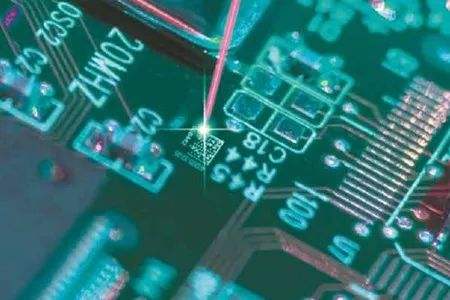
As for the verification of the finished circuit board, because the circuit board manufacturing process checkpoints are cumbersome, in order to make the product more sophisticated and reduce the number of defective parts, the process equipment should be regularly maintained and cleaned to maintain stable production conditions, and the production must be in a high-cleanliness environment. To avoid errors in the finished product.
The board processing is a multi-channel chemical liquid immersion and processing operation. The equipment must maintain automatic temperature, timing and fixed speed processing of materials. At the same time, the process needs to add chemicals at any time according to the pH value of the liquid material to maintain the composition stability of the chemical immersion material.
In addition to the standardization of the manufacturing process to maintain product quality, product quality must also rely on a high-cleanliness environment to avoid material contamination. For example, the production line can be processed in a dust-free environment, and the liquid photoresist production line must be equipped with dust filtering and board surface dust removal conditions. Perform PCBA processing.
Production is to pay close attention to processing at all stages to maintain consistent quality and reduce production defects
In order to maintain the output quality of the back-end workpieces, quality issues must not be ignored in the process treatment of each PCBA processing section. Defects in the process and the quality of the final product will also be greatly affected. Each stage of the manufacturing process needs to implement first product testing, final product testing, and intermediate product sampling monitoring to maintain product PCBA processing quality supervision.
In the drilling process, a pin-guage can be implemented to check the hole diameter status to verify the quality of the first product. The electroplating process can use a palm-type hole copper thickness gauge to check the thickness of the copper plating, and check the copper density of the hole with a slice The bonding condition with the inner layer ensures the quality of plated holes. After the copper plated plate is edging, the glass fiber, resin, and dust are removed, the copper surface is leveled and the copper bumps and dents are removed with an abrasive belt machine.
At the same time, high-volume production is equipped with machine vision assistance, supplemented by automatic optical conveyor belts for workpiece inspection, and the inter-layer alignment of the multilayer board can be matched with X-Ray to confirm the alignment accuracy. In addition, automatic optical inspection can be used for comparison and analysis of original circuit drawings to prevent fixed disconnection, circuit short circuit or circuit gap problems of the workpiece.
After pickling, brushing, and microetching of bare copper in the solder mask process, the oxide layer and micro copper powder on the copper surface need to be removed, and the roughness of the copper foil surface itself can be increased to improve the adhesion of the ink solder mask., While improving the ability to protect the circuit board. In the printing stage, the ink uniformity can be inspected visually. After the circuit board is baked, the thickness of the coated ink must be measured with a film thickness meter.
In the multi-layer board pressing stage, the key is temperature and pressure control. To achieve the best pressing, two-stage processing can be used to extend the two-stage hot pressing time to strengthen the hardness, flatness and copper of the board. The adhesion of the foil. The final circuit board product verification can generally be output by CAM Data, and use the automatic fixture software to construct the production program of the fixture, and quickly detect and select defective workpieces through the fixture.