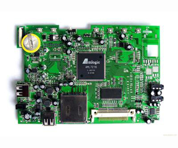
PCBA labor and materials is a one-stop service, which contains many links, and each link will have an impact on the quality of the final product. Let’s talk about several important nodes in PCBA labor and materials to ensure quality:
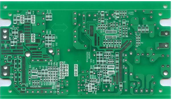
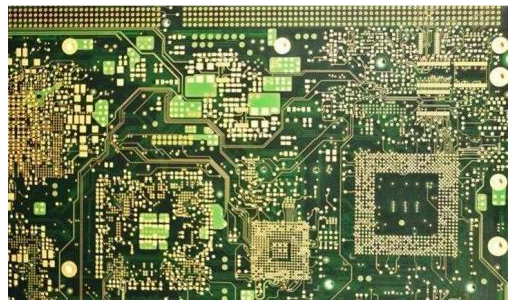
1. SMT patch processing
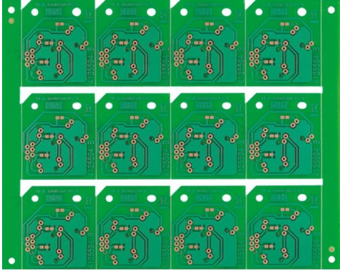
The details of the systematic quality control of solder paste printing and reflow soldering temperature control in SMT chip processing are key nodes in the PCBA manufacturing process. At the same time, for the printing of high-precision circuit boards with special and complex processes, laser stencils need to be used according to specific conditions to meet higher quality and processing requirements. According to PCB manufacturing requirements and customer product characteristics, some may need to increase U-shaped holes or reduce steel mesh holes. The steel mesh needs to be processed according to the requirements of PCBA processing technology.

Among them, the temperature control accuracy of the reflow oven is very important for the wetting of the solder paste and the firmness of the stencil welding, and can be adjusted according to the normal SOP operation guide. In order to minimize the quality defects of PCBA patch processing in the SMT link. In addition, strict implementation of the AOI test can greatly reduce the defects caused by human factors.
Two, DIP plug-in post welding
DIP plug-in post soldering is the most important and final process in the circuit board processing stage. In the process of DIP plug-in post-welding, the consideration of the furnace jig for wave soldering is very important. How to use the furnace fixture to greatly increase the yield rate, reduce soldering defects such as continuous tin, little tin, and tin shortage, and according to the different requirements of customers’ products, PCBA processing plants must continue to summarize experience in practice, The process achieves technological upgrading.
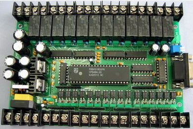
Three, test and program firing
The manufacturability report is an evaluation work that we should do before the entire production after receiving the customer’s production contract. In the previous DFM report, we can provide some suggestions to the customer before the PCB processing. For example, some key test points are set on the PCB (test point) for the key test of the continuity and connectivity of the circuit after the PCB soldering test and the subsequent PCBA processing. When conditions permit, you can communicate with the customer to provide the back-end program, and then burn the PCBA program into the core master IC through the burner. In this way, the circuit board can be tested more concisely through touch action, so that the integrity of the entire PCBA can be tested and inspected, and defective products can be found in time.
Four, PCBA test
In addition, many customers who are looking for PCBA package labor and materials one-stop service also have requirements for PCBA back-end testing. The content of this kind of test generally includes ICT (circuit test), FCT (function test), burn test (aging test), temperature and humidity test, drop test, etc.