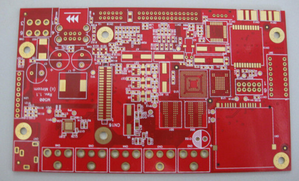
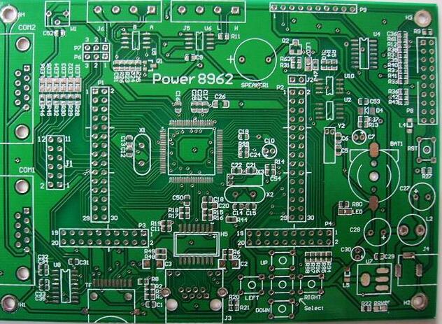
PCBA processing belongs to high-precision manufacturing and must comply with relevant actual operating rules. So, what should be paid attention to in PCBA processing? Next, let me introduce you:
1. During PCBA processing, the surface to be soldered cannot be taken with bare hands, because the grease secreted by human hands will reduce solderability and easily lead to soldering defects.
2. Smoking is prohibited in the PCBA work area, and no sundries that are not related to work are placed, and the workbench is kept clean and tidy.
3. It is forbidden to stack PCBA boards to avoid physical damage; special brackets should be configured and placed according to the type.
4. Regularly inspect the EOS/ESD workbenches to confirm that they can work normally, to avoid various hazards caused by incorrect grounding methods or oxides in the ground connection parts. Special attention should be given to the joints of the "third line" grounding terminal. protect.

5. In PCBA processing, the operating rules should be strictly followed to ensure the final quality of the product, reduce component damage and reduce costs.
6. Do not use skin-protecting oils to coat hands or various silicone-containing detergents, otherwise it will cause problems in solderability and adhesion performance of conformal coatings.
7. Components sensitive to EOS/ESD must be marked with appropriate EOS/ESD marks to avoid confusion with other components.
8. The operation steps for PCBA and components are reduced to a minimum to prevent danger.
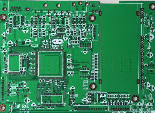
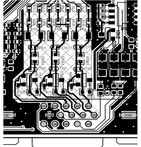
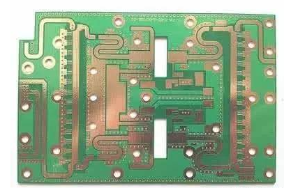
Why is the PCB circuit board distorted during PCBA processing?
PCB board distortion is a problem that may occur in PCBA mass production. It will have a considerable impact on placement and testing. Therefore, this problem should be avoided in production. Generally speaking, the reasons for PCB distortion are as follows:
1. Improper selection of the raw materials of the PCB itself, such as the low T of the PCB, especially the paper-based PCB, whose processing temperature is too high, and the PCB becomes bent.
2. Unreasonable PCB design and uneven distribution of components will cause excessive thermal stress on the PCB. Larger connectors and sockets will also affect the expansion and contraction of the PCB, resulting in permanent distortion.
3. PCB design problems, such as double-sided PCB. If the copper foil on one side is too large, such as a ground wire, and the copper foil on the other side is too small, this will also cause uneven shrinkage on both sides and deformation.
4. Improper use of fixtures or too small distance between fixtures, for example, if the middle finger grip of wave soldering is too tight, the PCB will expand and deform due to the soldering temperature.
5. Excessive temperature during reflow soldering can also cause PCB distortion.
For the above reasons, the engineer proposed corresponding solutions:
1. When price and space permit, choose PCB with high Tg or increase PCB thickness to obtain the best aspect ratio.
2. Design the PCB reasonably. The area of the double-sided steel foil should be balanced, and the copper layer should be covered in the place where there is no circuit, and appear in the form of a grid to increase the rigidity of the PCB;
3. Pre-bake the PCB before mounting, the condition is 125 degree Celsius/4h.
4. Adjust the clamp or clamping distance to ensure the space for PCB thermal expansion.
5. The temperature of the welding process should be adjusted as low as possible; a slight distortion has occurred, and it can be placed in a positioning fixture and heated and reset to release the stress. Generally, satisfactory results will be achieved.