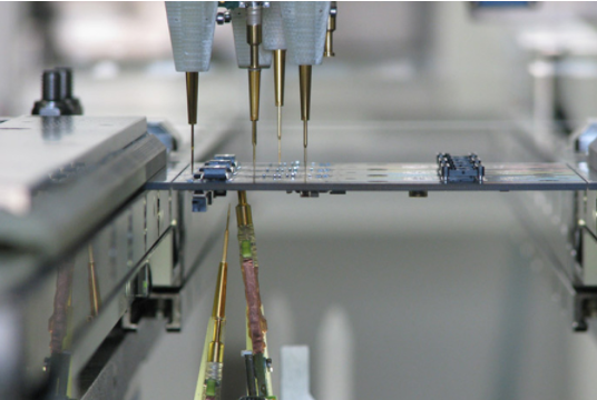
As we all know, SMT chip processing has requirements for PCB design. Only PCB boards designed with reasonable specifications can give full play to the processing capabilities of SMT chip equipment and realize efficient PCBA processing.
SMT chip processing requirements for PCB design
The requirements of SMT patch processing for PCB design include: shape, size, thickness, positioning hole, process edge, fiducial mark, and board.
1. PCB shape
PCB is generally rectangular, and the best aspect ratio is 3:2 or 4:3. When the aspect ratio is large, it is easy to warp and deform. It is recommended to standardize the PCB size as much as possible to simplify the processing process and reduce the processing cost.
2. PCB size
Different SMT equipment has different requirements for PCB size. When designing PCB, the maximum and minimum mounting size of SMT equipment must be considered. The general size is 50*50~350*250mm (the latest SMT equipment has a larger PCB size. For example, the maximum PCB size of Universal’s Genesis GX reaches 813*610mm).

3. PCB thickness
The thickness of the PCB should consider the mechanical strength requirements of the PCB and the weight of the components per unit area of the PCB, generally 0.3~6mm. The thickness of the commonly used PCB is 1.6mm, the extra-large board can be 2mm, and the microstrip board for radio frequency is generally 0.8~1mm.
SMT chip processing
4. PCB positioning hole
Some SMT equipment (such as placement machines) use hole positioning. In order to ensure that the PCB can be accurately fixed on the equipment fixture, the PCB is required to reserve positioning holes. Different devices have different requirements for positioning holes. Generally, a pair of positioning holes are required in the lower left corner and the lower right corner of the PCB. The hole diameter is Φ4mm (there are also Φ3mm or Φ5mm). The wall of the hole is not allowed to be metalized. One of the positioning holes is also acceptable Designed as an oval hole for quick positioning. Generally, the distance between the main positioning hole and the two sides of the PCB is 5mm*5mm, and the distance between the adjustment hole and the bottom of the PCB is 5mm. SMD components are not allowed within 5mm around the positioning hole.
5. PCB process side
In the SMT production process, the PCB is completed by track transmission. In order to ensure that the PCB is reliably fixed, a size of 5mm is generally reserved on the side of the transmission track (long side) to facilitate the clamping of the equipment. Mounting is not allowed within this range. Device. When it cannot be reserved, the process edge must be added. For some plug-in products that have been wave soldered, generally the side (short side) needs to reserve a size of 3mm in order to block the tin strip.
6. PCB fiducial mark (Fiducial Mark)
The reference point is also called Mark, which provides a common measurable point for all steps in the SMT assembly process, ensuring that each device used in the assembly can accurately locate the circuit pattern. Therefore, the Mark point is very important for SMT production. Mark points are generally divided into whole board Mark, jigsaw Mark, and partial recognition Mark (foot spacing ≤0.5mm). Generally, the mark point in the center of the Mark point is metal copper foil, with a diameter of 1.0mm, and the surrounding open contrast area has a diameter of 3mm, and metal copper The color contrast between the foil and the surrounding open area should be obvious. Silk screen, pad or V-Cut etc. are not allowed within the range of Φ3mm.
7. PCB board design
General principle: When the size of the PCB single board is less than 50mm*50mm, it must be assembled. It is recommended that when the size of the PCB is less than 160mm*120mm, the panel design should be used to convert it to an ideal size that meets the production requirements for plug-in and soldering, and improve production efficiency and equipment utilization. But note that the size of the jigsaw puzzle should not be too large, and it must meet the requirements of the equipment. V-shaped grooves, stamp holes or punching grooves can be used between the panels. It is recommended that the same board use only one method of splitting.
For part of the double-sided SMD boards assembled on the entire surface, the yin and yang imposition design can be adopted, so that the same stencil can be used, saving programming time and improving production efficiency. However, for larger and heavier devices, the restrictions are as follows: A=device weight/contact area between pins and pads.
SMT chip processing
The above is an introduction to the requirements of SMT chip processing for PCB design.