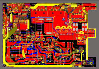
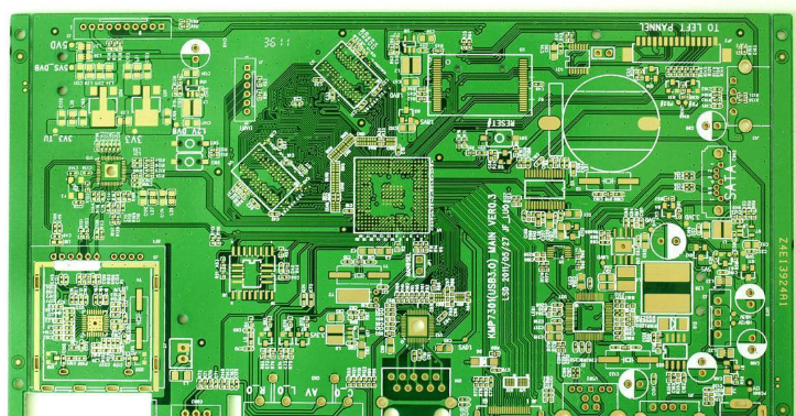
What is the process frombare PCB to PCBA, let’s explain in detail below:
1. SMT placement process
SMT (Surface Mounted Technology) is a surface mount technology (Surface Mounted Technology), which is one of the most popular technologies and processes in the electronics assembly industry.
Simply put, it is a kind of surface mount components without leads or short leads (SMC/SMD for short, chip components in Chinese) mounted on the surface of a Printed Circuit Board (PCB) or the surface of other substrates On the other hand, the circuit assembly technology of soldering and assembling by methods such as reflow soldering or dip soldering.
So what preparations need to be made before SMT placement?
1. There must be a MARK point on the PCB, also called a reference point, which is convenient for the placement of the placement machine and is equivalent to a reference object;
2. To make a stencil to help the deposition of solder paste, transfer the exact amount of solder paste to the exact position on the empty PCB;

3. SMD programming, according to the provided BOM list, the components are accurately positioned and placed in the corresponding position of the PCB through programming.
After all the above preparations are completed, SMT patch can be carried out.
First of all, the placement machine determines whether the board is in the correct direction according to the MARK point on the board that is sent in, and then the solder paste is brushed on the stencil, and the solder paste is deposited on the PCB pads through the stencil.
Next, the placement machine places the components on the corresponding positions of the PCB board according to the placement programming, and then undergoes reflow soldering to effectively contact the components, solder paste and the circuit board.
Finally, automatic optical inspection is carried out to check the components on the PCB board, including: virtual soldering, solder connection, device orientation, etc., but the functional inspection cannot be done because the board has plug-in components that have not been soldered.
It should be noted that some devices have positive and negative poles or pin order, so it is necessary to check the incoming materials to prevent patch errors, especially for BGA packaged devices. If the direction is wrong, subsequent disassembly and repair soldering are compared Time-consuming and laborious.
Second, the DIP plug-in process
DIP (Dual in-Iine Package) is the English abbreviation for dual in-line package. In fact, it is a device that can be perforated and welded on the PCB board, commonly known as plug-in components.
What preparations need to be done before DIP plug-in?
1. Prepare the furnace fixture and fix the PCB board to facilitate the transmission on the conveyor belt;
2. Need to correct the pins of plug-in devices with too long pins to a proper length;
3. Manpower is required to insert the plug-in device into the via hole of the corresponding PCB.
Next, briefly describe the process of DIP plug-in: The DIP plug-in process is much simpler than the SMT patch process, but it requires human assistance to insert the plug-in component into the corresponding hole, and then pass through the wave soldering machine, the plug-in device is perfectly welded On the PCB board.
Some people may worry, isn't the solder in the solder pool splashed all over the board?
The answer is no. The solder in the solder pool will only stick to the place where it is in contact with the metal and will not stick to the green solder mask. This is the role of the solder mask.
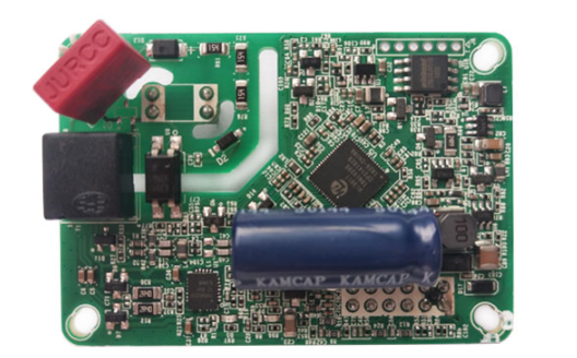
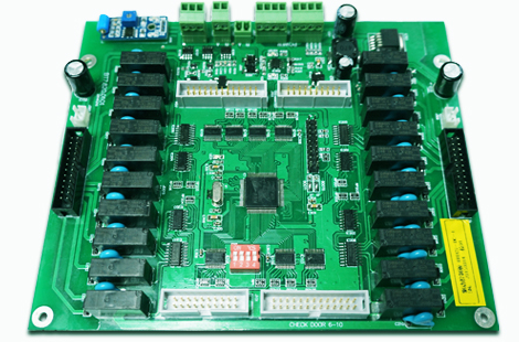
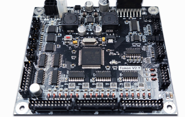
After the plug-in device is soldered, is the PCBA completed? Of course not, because the board after the patch and plug-in is also checked and functionally verified.
3. Perform functional testing on the produced PCBA
The functional test of the produced PCBA can be divided into two steps:
The first step: human visual inspection of PCBA, preliminary screening of defective boards, such as: tin connection, false soldering, missing soldering and other visible errors with the naked eye, and then send the defective board for repair, the board with no problem will enter the second step.
Step 2: Check the PCBA with the test fixture, which is actually the power-on test function of the PCBA. Use the test on the test fixture to do the corresponding test for the corresponding test point of the PCBA, such as: power on and off, relay pull-in, communication, etc., judge Whether each small module on the board can work normally.
After the above two steps of screening, not only the problem board can be screened out, but also the problem of the problem board can be determined during the screening process, which reduces a certain amount of work for subsequent repairs of the problem board.
Therefore, it can be seen that in the process from PCB bare board to PCBA, technicians conduct strict and comprehensive tests on every step, just to ensure that every step in the product production process is normal. Only in this way can we continue. step.
4. Waterproof, dustproof and anti-corrosion treatment for PCBA
Water-proof, dust-proof and anti-corrosion treatment is to spray or dip wax on PCBA. Each company may have its own way of processing, some manually apply the three-proof paint, some machines spray the three-proof paint, some dip wax, and of course some do not do the treatment.