What are the basic principles of PCBA design for manufacturability?
1. Optimum surface mounting and crimping components.
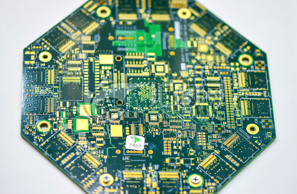
Surface mount components and crimping components have good manufacturability. With the development of component packaging technology, most components can be purchased in packaging categories suitable for reflow soldering, including plug-in components that can be soldered by through-hole reflow soldering. If the design can achieve full surface assembly, it will greatly improve the efficiency and quality of assembly. Crimping components are mainly multi-pin connectors. This type of package also has good manufacturability and connection reliability, and is also a preferred category.
2. For PCBA assembly.

The package size and pin pitch are considered as a whole. The package size and pin pitch have the greatest impact on the overall board manufacturability. Under the premise of selecting surface mount components, a set of packages with similar processability or suitable thickness stencils for solder paste printing must be selected for PCBs of specific size and assembly density. For example, for mobile phone boards, the selected packages are suitable for soldering and printing with 0.1mm thick steel mesh.
3. Shorten the process path The shorter the process path, the higher the production efficiency and the more reliable the quality.
The preferred process path design is:
(1) Single-sided reflow welding;
(2) Double-sided reflow welding;
(3) Double-sided reflow soldering + wave soldering;
(4) Double-sided reflow soldering + selective wave soldering;
(5) Double-sided reflow welding + manual welding.
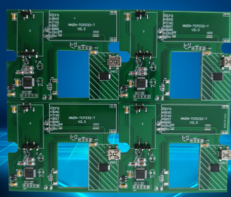
4. Optimize the layout of components
Component layout design mainly refers to the layout and spacing design of components. The layout of the components must meet the requirements of the welding process. A scientific and reasonable layout can reduce the use of bad solder joints and tooling, and can optimize the design of the steel mesh.
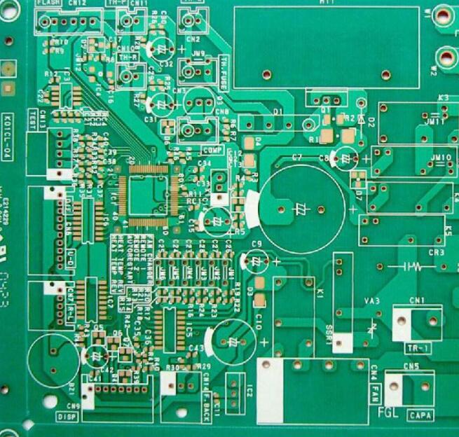
5. Consider the pad as a whole
The design pads of solder mask and stencil opening, and the design of solder mask and stencil opening determine the actual distribution value of solder paste and the formation process of solder joints. Coordinating the design of pad, solder mask and steel mesh has a great effect on improving the straight-through rate of welding.
6. Focus on new packaging
The so-called new package does not completely refer to the newly released package, but refers to those packages that the company has no experience in using. For the introduction of new packages, a small batch of process verification should be carried out. Others can use it, but it doesn't mean you can use it. The prerequisite for using it is to have done experiments, understand the process characteristics and potential problems, and master the countermeasures.
7. Focus on BGA, chip capacitors and crystal oscillators
BGAs, chip capacitors and crystal oscillators are typical stress-sensitive components. During layout, avoid placing them in places where PCB welding, assembly, workshop turnover, transportation, and use are prone to bending and deformation.
8. Study cases to improve design rules
Manufacturability design rules are derived from production practices. Continuous optimization and perfection of design rules based on the continuous occurrence of poor assembly or failure cases is of great significance for improving manufacturability design.