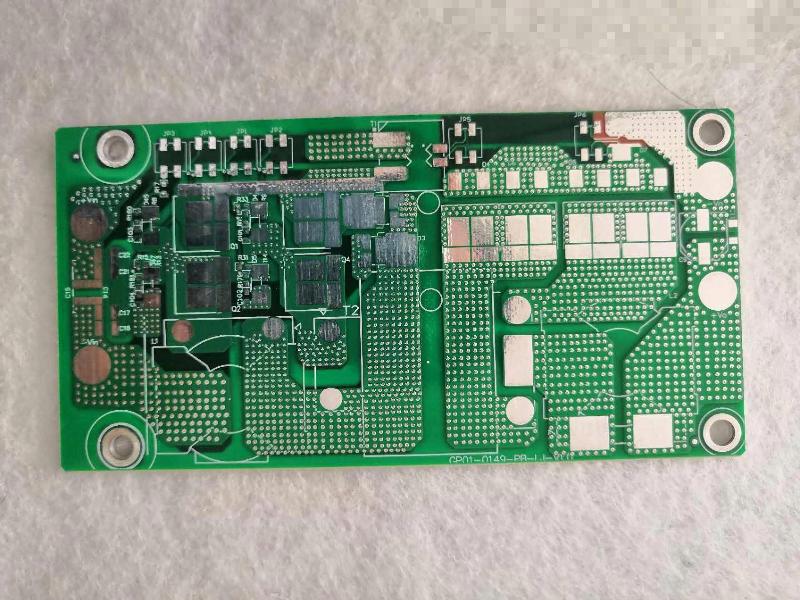
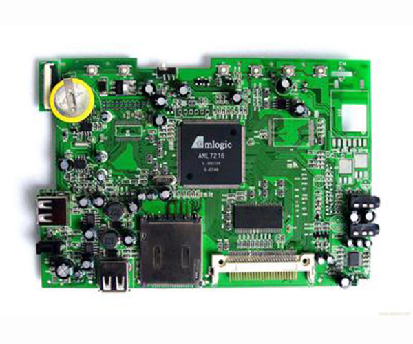
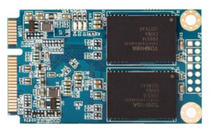
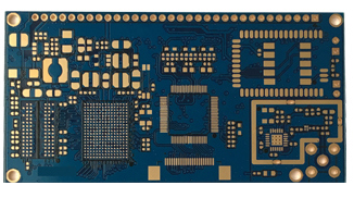
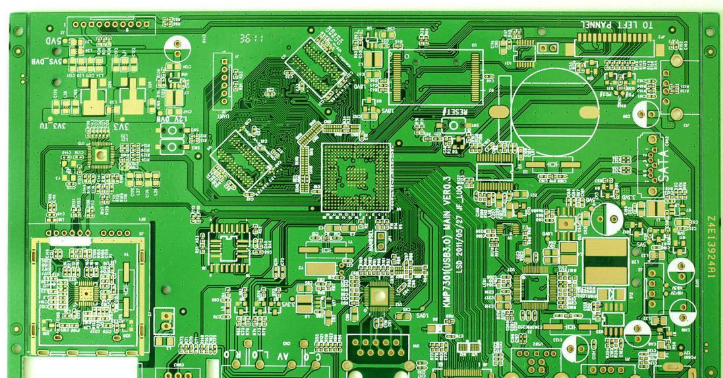
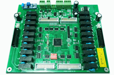
PCBA processing is the whole process of producing a finished electronic device after a complete set of processing steps such as PCB patterning, SMT patch processing, DIP software processing, quality inspection, testing, and assembly. There are many assembling methods.
One, single layer mixed
Commonly used circuit boards for assembly are single-layer PCBs. Single-layer mixed assembly means that SMT patches and DIP crimping components are distributed on a different side of the PCB. The soldering surface is a single side, and the patch surface is another single side. . This type of assembly method uses single-layer PCB and wave soldering methods. There are actually two assembly methods:
(1) Laying first and then inserting method: firstly mount the SMC/SMD on the B side of the PCB, and then crimp the THC on the A side.
(2) First insert and then paste method: that is, the THC is crimped on the A side of the PCB first, and then the SMD is installed on the first layer of the B side.
Two, mixed on both sides
Commonly used circuit boards for assembly of this type of PCBA processing are double-sided PCBs. SMT patch and DIP software can be mixed and distributed on the same side or both sides of the PCB. In this type of assembly method, there is also a difference between laying first and sticking SMC/SMD later. Generally, the selection is based on the type of SMC/SMD and the size of the PCB. Generally, the first paste method is more preferred. Two common assembly methods of this kind:

(1) SMT components and DIP components are on the same side: SMT patch components and DIP software components are on the same side of the PCB; DIP software components are on one or both sides. Generally, SMC/SMD is laid first and then software DIP is used in this category.
(2) DIP components have SMT components on one side and both sides: put the surface mount integrated integrated IC (SMIC) and THT on the A side of the PCB, and put the SMC and small design transistor (SOT) on the A side of the PCB. B side.
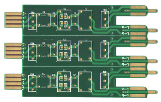
3. Full surface assembly
The assembled circuit boards processed by this type of PCBA are single-layer and double-sided PCBs, and there are only SMT components on the PCB and no THT components. Because electronic devices have not yet completed SMT at this stage, there are few such assembly methods in specific applications. There are two assembly methods for this:
(1) Single-layer surface assembly.
(2) Two-sided surface assembly.
The characteristics of surface mount components in PCBA processing are as follows:
1. On the electrodes of SMT components, some welding ends have no leads at all, and some have very small leads; the distance between adjacent electrodes is much smaller than the lead distance, and the distance between the pins of the integrated circuit is reduced to 0.3 mm; Under the same integration level, the area of SMT components is smaller, and the chip resistance and capacitance have been reduced to 0.6mm 0.3mm.
2. The SMT component is directly mounted on the surface of the printed circuit board, and the electrode is soldered on the pad on the same side of the SMT component. In this way, there are no pads around the through holes, which greatly increases the wiring density.
3. During PCBA processing, the surface mount technology not only affects the area occupied by the wiring on the printed circuit board, but also affects the electrical characteristics of the devices and components. There is no lead or short lead, which reduces the parasitic capacitance and inductance of the components, thereby improving the high-frequency characteristics, which is beneficial to increase the frequency of use and the speed of the circuit.
4. The shape is simple, the structure is sturdy, and it is close to the surface, which enhances the reliability and impact resistance; when assembling, there is no lead bending or trimming. When the printed circuit board is manufactured, the size and shape of the through hole for placing the component are standardized and reduced, and the automatic placement can be performed by using an automatic placement machine. The method has high efficiency, high reliability, convenient mass production, and low comprehensive cost.
5. In the traditional sense of PCBA processing, surface mount components have no leads or short leads. The entire surface component can withstand higher temperatures, but the pins or endpoints of surface mount components can withstand lower temperatures during soldering.