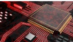
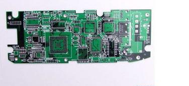
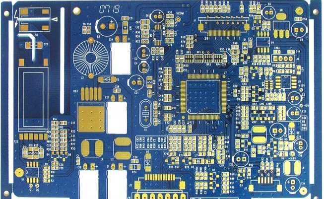
PCBA is made on the empty PCB board through SMT, and then through the production process of DIP plug-in. It will involve a lot of fine and complicated process and some sensitive components. If the operation is not standardized, it will cause process defects or components. Damage, affecting product quality and increasing processing costs. Therefore, in the PCBA patch processing, it is necessary to comply with the relevant operating rules and operate in strict accordance with the requirements. The following is an introduction for everyone.
The operating rules of PCBA patch processing:
1. There should not be any food or drink in the PCBA work area, smoking is prohibited, no sundries not related to work should be placed, and the workbench should be kept clean and tidy.
2. The surface to be soldered during PCBA patch processing cannot be taken with bare hands or fingers, because the grease secreted by human hands will reduce solderability and easily lead to soldering defects.

3. The operation steps for PCBA and components are reduced to a minimum to prevent danger. In assembly areas where gloves must be used, soiled gloves can cause contamination, so gloves must be replaced frequently when necessary.
4. Do not use skin-protecting oils to coat hands or various silicone-containing detergents, as they can cause problems in solderability and conformal coating adhesion. A specially formulated detergent for PCBA soldering su
The concept and meaning of PCBA mixing degree
1, background description
In IPC-SM-782, there are two important concepts "Producibility Levels" (producibility level) and "Component Mounting Complexity Levels" (component mounting complexity level), they are different but they are divided into three levels and correspond. These two concepts are used to describe the complexity of PCBA assembly. The three-level division is based on the technology used in assembly-through-hole insertion technology, surface assembly technology and mixed mounting technology.
These two concepts are not completely consistent with reality. On the one hand, the use of plug-in components is becoming less and less; on the other hand, the difficulty and complexity of the same-side assembly of ordinary and fine-pitch packages has far exceeded the mixed application of plug-in technology and surface assembly technology. The difficulty and complexity brought about. That is to say, the complexity of today's electronic manufacturing mainly comes from two challenges: one is the smaller and smaller component package size; the other is the mixed use of ordinary and fine-pitch packages on the same mounting surface of the PCB. This is also the biggest challenge facing PCBA manufacturability design today. The core task of PCBA manufacturability design is to solve the problem of mixing ordinary and fine-pitch packages on the same mounting surface through packaging selection and component layout design methods.
2, mixing degree
The degree of mixing is an important concept proposed in this book. It refers to the degree of difference in the assembly process of various packages on the PCBA mounting surface. Specifically, the degree of difference between the process methods used in the assembly of various packages and the thickness of the stencil, and the assembly process requirements The greater the degree of difference, the greater the degree of mixing, and vice versa. The greater the degree of mixing, the more complicated the process and the higher the cost.
The degree of PCBA mixing reflects the complexity of the assembly process. The PCBA that we usually talk about "good soldering" actually contains two layers. One layer means whether there are components on the PCBA with a narrow process window, such as fine-pitch components; the other layer means the PCBA mounting surface The degree of difference in various packaging and assembly processes.
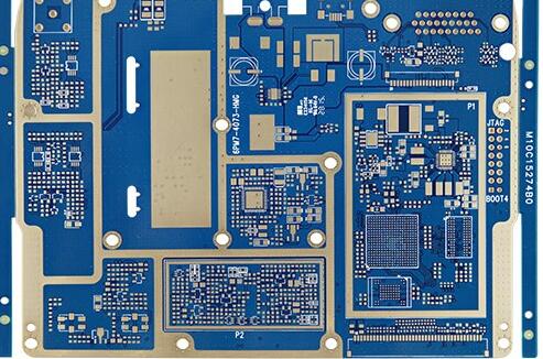
The higher the mixing degree of PCBA, the more difficult it is to optimize the assembly process of each type of package and the worse the manufacturability. To give an example, such as mobile phone PCBA, although the components used on the mobile phone board are fine pitch or small-sized components, such as 01005, 0201, 0.4mmCSP, PoP, the assembly of each package is very difficult, but their craftsmanship The requirements belong to the same level of complexity, the degree of mixing of the processes is not high, each packaging process can be optimally designed, and the final assembly yield will be very high. The communication PCBA, although the components used are relatively large, the degree of mixing of the process is relatively high, and the ladder steel mesh is required for assembly. Limited by the component layout gap and the difficulty of making steel mesh, it is difficult to meet the individual needs of each package. The final process plan is often a compromise solution that takes care of various packaging process requirements, rather than the optimal solution. The rate will not be very high. This is the significance of proposing the concept of mixing degree.
Packages with similar installation process requirements on the same assembly surface are the basic requirements for package selection. In the hardware design stage, establishing a suitable package is the first step in design for manufacturability.
3. Measurement and classification of mixing degree
The degree of mixing of PCBA is expressed by the maximum difference of the ideal stencil thickness of the components used on the same assembly surface of the PCB. The larger the difference, the greater the degree of mixing and the worse the manufacturability.
The greater the thickness difference of the steel mesh, the more difficult it is to optimize the process. The difficulty of the process is not to say that the production of the step stencil is difficult, but the greater the thickness of the step stencil, the more difficult it is to guarantee the printing quality of the solder paste. Ideally, the step thickness of the step steel mesh should not exceed 0.05mm (2mil)
4, the relationship between the component pin spacing and the maximum thickness of the steel mesh
The thickness of the steel mesh is mainly considered from two aspects, namely, the coplanarity of the component pin pitch and the package. There is a certain correspondence between the component pin spacing and the area of the steel mesh window, which basically determines the maximum thickness value that can be used, and the coplanarity of the package determines the minimum thickness value that can be used. Since the thickness of the stencil is not designed according to the pin pitch of a single component, the degree of mixing cannot be simply judged according to the pitch, but it can be used as a basic reference for component packaging selection.
This article introduces in detail about the PCBA mixing degree, the greater the mixing degree, the more complicated the process, and the higher the cost.
rface is available.
5. Components and PCBA sensitive to EOS/ESD must be marked with appropriate EOS/ESD marks to avoid confusion with other components. In addition, in order to prevent ESD and EOS from endangering sensitive components, all operations, assembly and testing must be completed on a workbench that can control static electricity.
6. Regularly check EOS/ESD workbenches to confirm that they can work normally (anti-static). The various dangers of EOS/ESD components can be caused by incorrect grounding methods or oxides in the ground connection parts. Therefore, special protection should be given to the "third line" grounding terminal joints.
7. It is forbidden to stack PCBA, otherwise physical damage will occur. There should be various types of special brackets on the assembly work surface, and they should be placed according to the type.
In the PCBA patch processing, these operating rules should be strictly followed, and the correct operation can ensure the final use quality of the product, and reduce the damage of the components and reduce the cost.