As HDI boards adapt to the development of high-integration IC and high-density interconnect assembly technology, PCB manufacturing technology has reached a new level. Become one of the hot spots of PCB manufacturing technology! People engaged in CAM production in various PCBCAM productions agree that the shape of HDI mobile phone boards is complicated. CAM with high line density is difficult to complete quickly and accurately! Facing customers' requirements for high quality and fast delivery, PCB has gained a little experience through continuous practice. I want to share with your circuit board.
How to define SMD is a difficult point produced by CAM.
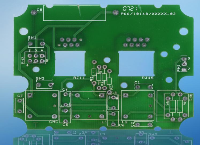
In the PCB production process, factors such as graphic transfer and etching will affect the final image, so we follow the customer's acceptance criteria in CAM production. Need compensation line and SMD. If we incorrectly define SMD finished products, some SMDs may be too small. Customers usually design 0.5 mm CSP on HDI mobile phone boards, the pad size is 0.3 mm, and some CSP pads have blind holes. The disk corresponding to the blind hole is also 0.3 mm, so that the CSP disk overlaps or crosses the blind hole. In this case, you must be careful to prevent mistakes. Take GENESIS2000 as an example).
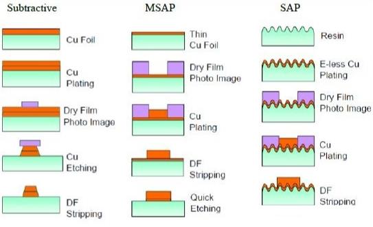
Traditional multi-layer board process and technology.

Cutting-inner layer manufacturing-oxidation treatment-lamination-drilling-hole plating (can be divided into full board and pattern plating)-outer coating-shape addition
Note 1: Inner layer production refers to the process of plate making, pattern transfer, film forming exposure, development, etching, and film release inspection after the material is opened.
Note 2: Outer layer production refers to the process of plate making-pattern transfer (film-forming exposure), etching and de-filming through hole plating.
(Note 3). Surface coating (plating) refers to the solder mask and character-coating (such as HALOSP chemical NI/Au chemical AG chemical Sn) after the outer layer is produced.
2.1 Meta equipment processing requirements.
2.1.1 The solderability of the component must be processed before the component is inserted. If the soldering ability is poor, the pins of the parts should be tinned first.
2.1.2 The component pin * pin pitch is consistent with the corresponding pad hole pitch of the PCB board..
2.1.3 The shape of the component pins should be conducive to the heat dissipation during the soldering process and the mechanical strength after soldering.
2.2 yuan equipment is required during the PCB board insertion process.
The order of inserting 2.2.1 components on the PCB is first low, then high, then light, then easy, and then special components. The installation of the previous process will not affect the installation of the next process.
After inserting and installing the 2.2 components, the logo should be read as far as possible from left to right.
The polarity of the polar components should be installed in strict accordance with the requirements of the drawings.
2.2.4 The plug-ins of the components on the PCB board should be evenly arranged, and the diagonal and three-dimensional cross and overlapping arrangements are not allowed, and the high side and low side are not allowed. Long and short pins are also not allowed.
2.3 Process requirements for PCB solder joints.
2.3.1 The mechanical strength of the solder joints should be sufficient.
2.3.2 Welding is reliable to ensure electrical conductivity.
The surface of the welded joint should be smooth and clean.
One problem in the PCB industry is that customers tend to design green double-sided VIA holes, without windows, and no single-sided windows to handle this design.
The first thing to consider is the surface treatment of the PCB. If it is tin (HALS), the single-sided plug technology must be avoided because the depth of the single-sided plug is lower. It is easy to cause the appearance of the tin bead when spraying tin.
If it is other surface treatments, such as Immersion Gold, OSP, Silver, etc., single-sided plug holes are acceptable. Considering the above factors, then check the customer's green oil window design. If it is some windows, you should try to avoid using green oil to cover the hole and let the green oil enter the hole. Because this method can easily lead to sessi beads.
Combining the above two situations, a good treatment method is to allow 1≤2mil tin ring processing method* to be welcomed by PCB manufacturers. Of course, the oil plug here is for ordinary photosensitive oil, not for heat-curing single-sided PCB circuit boards.
Multi-layer steel plate spraying process.
The inner layer pattern and inner layer etching test of the positioning hole of the blanking edging drill, blackening-lamination drilling, heavy copper thickening, outer layer pattern, tin plating etching, tin removal, secondary drilling, inspection silk screen solder mask .