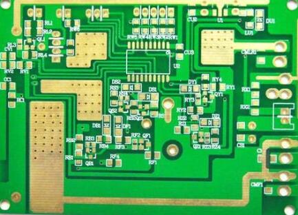
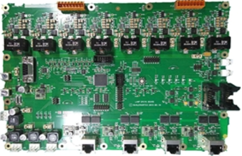
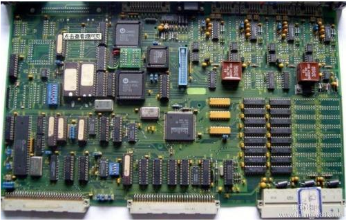
Experts summarize the characteristics, advantages and disadvantages of various surface processes produced by PCB surface treatment technology
The solderability of bare copper itself is very good, but it is easy to be oxidized. In order to ensure the good solderability and electrical properties of PCB products, technical experts have summarized the characteristics, advantages and disadvantages of various surface processes!
OSP
Main feature: Cover a layer of organic protective film on the copper surface
Thickness control: 0.2~0.6um
Advantages: uniform film thickness and low cost
Disadvantages: difficult to withstand multiple reflow soldering
Shen Yin
Main feature: A silver layer is covered on the copper surface through displacement reaction
Thickness control: 0.2~0.4um
Advantages: uniform silver layer, average cost, long storage period
Disadvantages: easy to oxidize, and it is difficult to completely solve the discoloration and yellowing of the silver surface, which affects the solderability

Shen Xi
Main feature: Cover a layer of tin on the copper surface through displacement reaction
Thickness control: ≥1.0um
Advantages: uniform tin layer, average cost, easy to aging
Disadvantages: the potion is easy to age, and the problem of tin whiskers is difficult to solve
Spray tin
Main features: through physical means, hot air leveling to obtain a protective layer
Thickness control: 2~40um
Advantages: solderability, best compatibility, long storage period
Disadvantages: lead, poor flatness
Lead-free spray tin
Main features: through physical means, hot air leveling to obtain a protective layer
Thickness control: 2~40um
Advantages: simple process, substitute for tin spraying, long storage period
Disadvantages: poor flatness, fluidity, poor solderability
Immersion Nickel Gold
Main feature: Cover a thin layer of nickel and gold on the copper surface through displacement reaction
Thickness control: 0.05~0.1um
Advantages: uniform coating, good solderability, long storage period
Disadvantages: high cost, plagued by black disk problems
Nickel Palladium
Main feature: Deposit a thin palladium layer before immersing gold
Thickness control: 0.05~0.1um
Advantages: suitable for wire bonding, reducing gold costs
Disadvantages: not widely adopted
Electric hard gold
Main feature: Cover a thin nickel-gold layer on the copper surface through electrochemical oxidation-reduction reaction
Thickness control: 0.38~2.0um
Advantages: wear resistance, oxidation resistance, low resistance
Disadvantages: poor solderability, high cost, used according to performance needs
Golden finger
Main feature: Cover a thin nickel-gold layer on the copper surface through electrochemical oxidation-reduction reaction
Thickness control: 0.25~1.5um
Advantages: wear resistance, oxidation resistance, low resistance
Disadvantages: poor solderability, high cost, used according to performance needs
Full board gold-plated
Main feature: Cover a thin nickel-gold layer on the copper surface through electrochemical oxidation-reduction reaction
Thickness control: 0.025~0.1um
Advantages: uniform coating, suitable for wire bonding
Disadvantages: high cost
The above is a summary of the surface treatment technology of PCB circuit boards