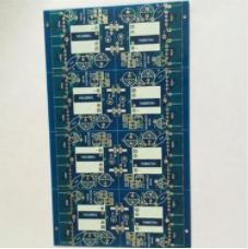
Printed circuit board are providers of electrical connections for electronic components and have a history of more than 100 years. According to the number of circuit board layers, printed circuit boards can be divided into single-sided boards, double-sided boards, four-layer boards, six-layer boards and other multilayer circuit boards. Today, printed circuit boards have reached a very fine level, and many techniques for improving and optimizing circuit boards have been born. The article mainly summarizes the key technology of printed circuit board manufacturing currently used, mainly including high-density interconnection circuit boards, high-density interconnection circuit boards of any layer, integrated printed circuit boards, high heat dissipation metal substrates, high-frequency and high-speed printed circuits The key technology of board and rigid-flex printed board manufacturing.
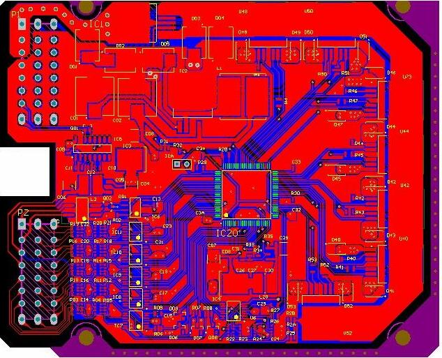
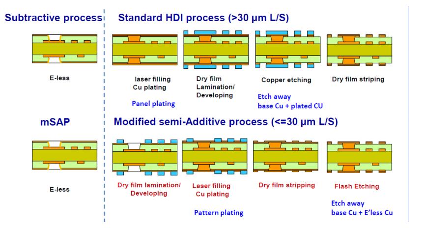
1. High-density interconnect circuit board
In the early 1990s, Japan and the United States pioneered the application of High Density Interconnect Technology (HDI). The manufacturing process used double-sided or multi-layer boards as the core board, and multi-layer stacking technology was used to maintain the layout of each level. Absolutely insulated PCB[4-5] to manufacture high-density, highly integrated electronic circuit boards. The five major characteristics of this type of circuit board are "miniature, light and thin, high frequency, fine, and heat dissipation." Continuous technological innovation based on the five characteristics is the development trend of today's high-density electronic circuit board manufacturing. "Thinning" determines the basis for the survival of high-density electronic circuits. Its birth directly led to and affected the production of fine and micro technology. Fine connecting wires, fine micro-drilling and the design of each layer of insulation determine whether the high-density electronic circuit board can adapt to high-frequency work and whether it is conducive to reasonable heat conduction. This is also an important method for judging the degree of integration of electronic circuits in ultra-high-density electronic circuit boards.

2. High-density arbitrary layer interconnection printed circuit board
For HDI with different hierarchical structures, there are big differences in process manufacturing. Generally, the more multi-layered structure, the more complex and precise it is, the more difficult it will be for manufacturing. At present, there are several major technological characteristics of the correlation between the board layers, namely "step connection", "wrong hole connection", "cross-layer connection" and "stacked hole connection", which will not be introduced in detail here. Ultra-high-density arbitrary-layer interconnected printed circuit boards are high-end products in printed circuit boards. Its biggest demand comes from the electronic product market that requires light, thin, and multi-functional characteristics, such as smart phones, notebook computers, digital cameras, and LCD TVs.
3. Integrated printed circuit board
Integrated printed circuit board technology is to integrate one or more separate electronic components (such as resistors, capacitors, capacitors, etc.) into a printed circuit board structure, so that the integrated printed circuit board has a certain degree of system function Printed circuit boards have the advantages of improving the reliability of electronic product system functions, improving signal transmission performance, effectively reducing production costs, and making the production process more green and environmentally friendly. It is a technical approach to the miniaturization of electronic device system integration and has huge advantages Market development potential. The system integration technology of embedding electronic components in printed boards has begun to enter the application stage abroad, and has made breakthroughs in related materials and manufacturing process technologies, and industry-leading foreign companies have begun to put this technology into mass production.
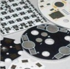
4. High heat dissipation metal substrate
High heat dissipation metal substrate mainly utilizes the better thermal conductivity of the metal substrate material itself to derive the heat source from the high-power components. Its heat dissipation performance is related to the structural layout of the multi-chip (component) package and the reliability of the component package. As a high-end printed board, the metal substrate with high heat dissipation is compatible with surface mount technology, reduces product volume, reduces hardware and assembly costs, replaces fragile ceramic substrates, increases rigidity, and obtains better mechanical durability. Power, showing strong competitiveness in many heat-dissipating substrates, and its application prospects are very broad. The buried (embedded) metal-based printed circuit board is a locally implanted metal block printed circuit board, which is a new type of heat dissipation PCB technology that has emerged in recent years. Its heat dissipation design concept is relatively advanced, and no public reports on related technologies have been found in domestic and foreign industry journals. As a heat dissipation substrate for high-power components, it has the following advantages due to the special design:
(1) Excellent heat dissipation performance, the components are in direct contact with the heat sink, and there is no heat dissipation bottleneck;
(2) Flexible design, which can fully meet the heat dissipation requirements of individual high-power components;
(3) Embedded design, coplanar with PCB, does not affect surface mount (SMD);
(4) Light weight and small size, in line with the mainstream development direction of light, thin, short and small electronic assembly;
(5) Compatible with PCB production process.
5. High frequency and high speed printed circuit board
High-frequency and high-speed printed circuits were used in the military field as early as the end of the 20th century. In the past ten years, part of the frequency bands of high-frequency communications originally used for military purposes have been given to civilian use, which has enabled civil high-frequency and high-speed information transmission technology to advance by leaps and bounds, and promoted the improvement of electronic information technology in all walks of life. It has the characteristics of long-distance communication, telemedicine surgery, and automatic control and management of large logistics warehouses. It should be pointed out that the electronic components and printed circuit board industries that work in high-frequency signal transmission have strict technical requirements, such as operating impedance range, metal connection smoothness, high-frequency and high-speed signal requirements for line width, and signal line and The relative distance between the strata, etc. Excellent process technology has driven the industrial development of electronic components and electronic products, and the demand is expected to reach more than 10 times in the next 5 years.
6. Rigid-flex printed board technology
In recent years, the high-performance, multi-functional, and compact and lightweight electronic equipment has shown an accelerated development momentum. Therefore, the requirements for miniaturization and high density of electronic parts and PCBs used in electronic devices are also increasing. In order to meet these requirements, innovations in the manufacturing technology of laminated multilayer boards for rigid (rigid) PCBs have prompted various laminated multilayer boards to be used in electronic devices. However, mobile devices such as portable devices and digital video cameras have not only accelerated the cycle of adding new functions or improving performance, but also have a strong tendency to be smaller, lighter and more prioritized. Therefore, the space given to the functional parts inside the case is only a limited and narrow space, which must be used effectively. In this case, a system structure composed of several small build-up multilayer boards and flexible boards (FPC) or cables connecting them is often used, which is called an analog rigid-flex PCB. Rigid-flex PCB also uses this combination and saves space. It is a functional composite multi-layer board that integrates several rigid PCBs and FPCs. Because it does not require connectors or space for connection, and has almost the same mountability as rigid PCB, rigid-flex PCBs are being widely used in mobile devices.