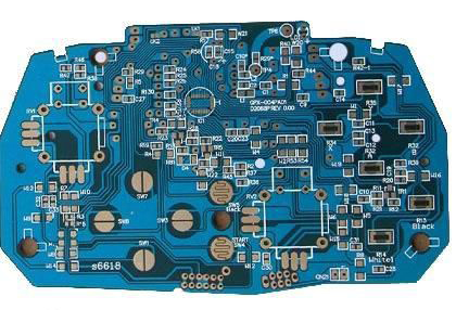
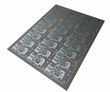
The key tasks of China's copper clad laminate (CCL) industry in the future development strategy, in terms of products, work hard on new PCB substratematerials, and through the development of new substrate materials and technological breakthroughs, China’s CCL cutting-edge technology has Promoted. The development of the new high-performance CCL products listed below is a key topic that engineers and technicians in China's copper clad laminate industry will pay attention to in future research and development.
Lead-free compatible copper clad laminate
At the European Union's October 11 meeting, two "European Directives" on environmental protection content were passed. They will formally implement the resolution on July 1, 2006. The two "European Directives" refer to the "Electrical and Electronic Product Waste Directive" (referred to as WEEE) and the "Restriction of the Use of Certain Hazardous Substances" (referred to as RoHs). In these two statutory directives, the requirements are clearly mentioned. The use of lead-containing materials is prohibited. Therefore, the best way to respond to these two directives is to develop lead-free copper clad laminates as soon as possible.

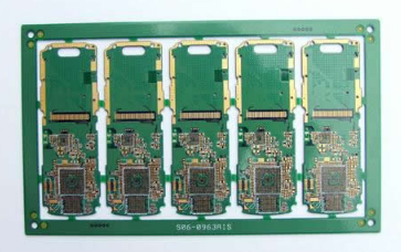
High performance copper clad laminate
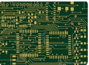
The high-performance copper clad laminates referred to here include low dielectric constant (Dk) copper clad laminates, copper clad laminates for high frequency and high speed PCBs, high heat resistance copper clad laminates, and various substrate materials (resin coated Copper foil, organic resin film that constitutes the insulating layer of multilayer PCB board with laminated method, glass fiber reinforced or other organic fiber reinforced prepreg, etc.). In the next few years (to 2010), in the development of this type of high-performance copper clad laminates, according to the forecasted future development of electronic installation technology, the corresponding performance index values should be reached.
Substrate material for IC package carrier
The development of substrate materials for IC packaging substrates (also known as IC packaging substrates) is currently a very important topic. It is also an urgent need to develop China's IC packaging and microelectronics technology. With the development of IC packaging in the direction of high frequency and low power consumption, IC packaging substrates will be improved in important properties such as low dielectric constant, low dielectric loss factor, and high thermal conductivity. An important subject of future research and development is the effective thermal coordination and integration of substrate thermal connection technology-heat dissipation.
In order to ensure the freedom of IC packaging design and the development of new IC packaging technology, it is indispensable to carry out model tests and simulation tests. These two tasks are very meaningful for mastering the characteristic requirements of substrate materials for IC packaging, that is, understanding and mastering its electrical performance, heat and heat dissipation performance, reliability and other requirements. In addition, it should further communicate with the IC packaging design industry to reach a consensus. The performance of the developed substrate material will be provided to the designer of the complete electronic product in time, so that the designer can establish an accurate and advanced data foundation.
The IC package carrier also needs to solve the problem of inconsistency in the coefficient of thermal expansion with the semiconductor chip. Even if it is a multi-layer PCB board suitable for the production of fine circuits, there is a problem that the thermal expansion coefficient of the insulating substrate is generally too large (generally, the thermal expansion coefficient is 60ppm/°C). The thermal expansion coefficient of the substrate reaches about 6 ppm, which is close to that of the semiconductor chip, which is indeed a "difficult challenge" for the manufacturing technology of the substrate.
In order to adapt to the development of high speed, the dielectric constant of the substrate should reach 2.0, and the dielectric loss factor can be close to 0.001. For this reason, a new generation of printed circuit boards that surpass the boundaries of traditional substrate materials and traditional manufacturing processes are predicted to appear in the world around 2005. The breakthrough in technology, first of all, is the breakthrough in the use of new substrate materials.